- 您現(xiàn)在的位置:買賣IC網(wǎng) > PDF目錄371757 > H1085E LDO Regulators PDF資料下載
參數(shù)資料
| 型號(hào): | H1085E |
| 英文描述: | LDO Regulators |
| 中文描述: | LDO穩(wěn)壓器 |
| 文件頁(yè)數(shù): | 3/5頁(yè) |
| 文件大?。?/td> | 57K |
| 代理商: | H1085E |

HI-SINCERITY
MICROELECTRONICS CORP.
Spec. No. : Preliminary Data
Issued Date : 1998.07.01
Revised Date : 1999.08.01
Page No. : 3/5
HSMC Product Specification
Applications Description
Output Voltage Adjustment
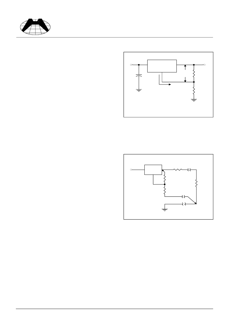
Like most regulators, the H1085E regulates the output
by comparing the output voltage to an internally generated
reference voltage. On the adjustable version, the V
REF
is
available externally as 1.25V between V
OUT
and ADJ. The
voltage ratio formed by R
1
and R
2
should be set to conduct
10mA (minimum output load). The output voltage is given
by the following equation : V
OUT
=V
REF
(1+R
2
/R
1
) + I
ADJ
R
2
On fixed versions of H1085E, the voltage divider is
provided internally.
Thermal Protection
H1085E has thermal protection which limits junction
temperature to 150
°
C. However, device functionality is
only guaranteed to a maximum junction temperature of
+125
°
C.
The power dissipation and junction temperature for H1085E in TO-220AB package given by
P
D
=(V
IN
- V
OUT
) I
OUT
, T
JUNCTION
=T
AMBIENT
+(P
D
x
θ
JA
), Note : T
JUNCTION
must not exceed 125
°
C
Current Limit Protection
H1085E is protected against overload conditions. Current protection is triggered at typically 4.5A.
Stability And Load Regulation
H1085E requires a capacitor from V
OUT
to GND to
provide compensation feedback to the internal gain stage.
This is to ensure stability at the output terminal. Typically, a
10uF tantalum or 50uF aluminum electrolytic is sufficient.
Note : It is important that the ESR for this capacitor does
not exceed 0.5
.
The output capacitor does not have a theoretical upper
limit and increasing its value will increase stability. C
OUT
=
100 uF or more is typical for high current regulator design.
H1085E load regulation is limited by the resistance of
the wire connecting it to the load(R
P
). For the adjustable
version, the best load regulation is accomplished when the
top of the resistor divider(R
1
) is connected directly to the
output pin of the H1085E. When so connected, R
P
is not
multiplied by the divider ratio. For fixed output versions,
the top of R
1
is internally connected to the output and ground pin can be connected to low side of the load as a
negative side sense if, so desired.
Thermal Consideration
The H1085E series contain thermal limiting circuitry designed to protect itself for over-temperature conditions.
Even for normal load conditions, maximum junction temperature ratings must not be exceeded. As mention in
thermal protection section, we need to consider all sources of thermal resistance between junction and ambient.
It contains junction-to-case, case-to-heat-sink interface and heat sink resistance itself. An additional heat sink is
applied externally sometimes. It can increase the maximum power dissipation. For example, the equivalent
junction temperature of 1A output current is 115
°
C without external heat sink. Under the same junction
temperature IC can operates 3A with an adequate heat sink. Therefore, to attach an extra heat sink is
recommended.
Junction-to-case thermal resistance is specified from the IC junction to the bottom of the case directly below the
die. The bonding wires are appending paths. The former is the lowest resistance path. Proper mounting is
required to ensure the best possible thermal flow this area of the package to the heat sink. Thermal compound at
the case-to-heat-sink interface is strongly recommended. The case of all devices in this series is electrically
connected to the output. Therefore, if the case of the device must be electrically isolated, a thermally conductive
spacer can be used, as long its thermal resistance is considered.
RL
R1
R2
Connect
R1 to Case
Connect
R2 to Load
Out
In
Adj
R
Parasitic
Line Resistance
V
IN
V
OUT
=V
REF
(1+R
2
/R
1
) + I
ADJ
R
2
V
IN
R1
R2
V
REF
In
Out
ADJ
I
ADJ
10uA
V
OUT
相關(guān)PDF資料 |
PDF描述 |
|---|---|
| H1092 | 10/100Base-T Quad Port Surface Mount Magnetics (5/01) |
| H1112 | 10/100Base-T Single Port Transformer Modules with Various Transmit Turns Ratios (12/00) |
| H1113 | 10/100Base-T Single Port Transformer Modules with Various Transmit Turns Ratios (12/00) |
| H1125 | 10/100Base-T Single Port Transformer Modules with Various Transmit Turns Ratios (12/00) |
| H1126 | 10/100Base-T Single Port Transformer Modules with Various Transmit Turns Ratios (12/00) |
相關(guān)代理商/技術(shù)參數(shù) |
參數(shù)描述 |
|---|---|
| H1085J | 制造商:HSMC 制造商全稱:HSMC 功能描述:3A LOW DROPOUT POSITIVE VOLTAGE REGULATOR |
| H1085U | 制造商:HSMC 制造商全稱:HSMC 功能描述:3A LOW DROPOUT POSITIVE VOLTAGE REGULATOR |
| H1086 | 功能描述:變壓器音頻和信號(hào) XFMR (SGL 1:1) RoHS:否 制造商:Skyworks Solutions, Inc. 頻率范圍:810 MHz to 960 MHz 初級(jí)線圈阻抗: 次級(jí)線圈阻抗: 絕緣電壓:23 dB 工作溫度范圍:- 40 C to + 85 C 端接類型:SMD/SMT 尺寸:6 mm L x 4.9 mm W x 1.6 mm H 產(chǎn)品:Splitters and Combiners |
| H108608C | 功能描述:電路板硬件 - PCB LINK PIN RoHS:否 制造商:Harwin 類型:Shield Clip 長(zhǎng)度:9.4 mm 螺紋大小: 外徑: 材料:Beryllium Copper 電鍍:Tin |
| H108614C | 制造商:Harwin 功能描述:PIN |
發(fā)布緊急采購(gòu),3分鐘左右您將得到回復(fù)。