- 您現(xiàn)在的位置:買賣IC網(wǎng) > PDF目錄371767 > HA5025IB (HARRIS SEMICONDUCTOR) Quad, 125MHz Video Current Feedback Amplifier PDF資料下載
參數(shù)資料
| 型號: | HA5025IB |
| 廠商: | HARRIS SEMICONDUCTOR |
| 元件分類: | 音頻/視頻放大 |
| 英文描述: | Quad, 125MHz Video Current Feedback Amplifier |
| 中文描述: | VIDEO AMPLIFIER, PDSO14 |
| 文件頁數(shù): | 6/13頁 |
| 文件大?。?/td> | 150K |
| 代理商: | HA5025IB |

6
Application Information
Optimum Feedback Resistor
The plots of inverting and non-inverting frequency response,
see Figure 8 and Figure 9 in the typical performance section,
illustrate the performance of the HA5025 in various closed
loop gain configurations. Although the bandwidth dependency
on closed loop gain isn’t as severe as that of a voltage
feedback amplifier, there can be an appreciable decrease in
bandwidth at higher gains. This decrease may be minimized
by taking advantage of the current feedback amplifier’s unique
relationship between bandwidth and R
F
. All current feedback
amplifiers require a feedback resistor, even for unity gain
applications, and R
F
, in conjunction with the internal
compensation capacitor, sets the dominant pole of the
frequency response. Thus, the amplifier’s bandwidth is
inversely proportional to R
F
. The HA5025 design is optimized
for a 1000
R
F
at a gain of +1. Decreasing R
F
in a unity gain
application decreases stability, resulting in excessive peaking
and overshoot. At higher gains the amplifier is more stable, so
R
F
can be decreased in a trade-off of stability for bandwidth.
The following table lists recommended R
F
values for various
gains, and the expected bandwidth.
PC Board Layout
The frequency response of this amplifier depends greatly on
the amount of care taken in designing the PC board. The
use of low inductance components such as chip resistors
and chip capacitors is strongly recommended. If leaded
components are used the leads must be kept short
especially for the power supply decoupling components and
those components connected to the inverting input.
Attention must be given to decoupling the power supplies. A
large value (10
μ
F) tantalum or electrolytic capacitor in
parallel with a small value (0.1
μ
F) chip capacitor works well
in most cases.
A ground plane is strongly recommended to control noise.
Care must also be taken to minimize the capacitance to
ground seen by the amplifier’s inverting input (-IN). The larger
this capacitance, the worse the gain peaking, resulting in
pulse overshoot and possible instability. It is recommended
that the ground plane be removed under traces connected to
-IN, and that connections to -IN be kept as short as possible to
minimize the capacitance from this node to ground.
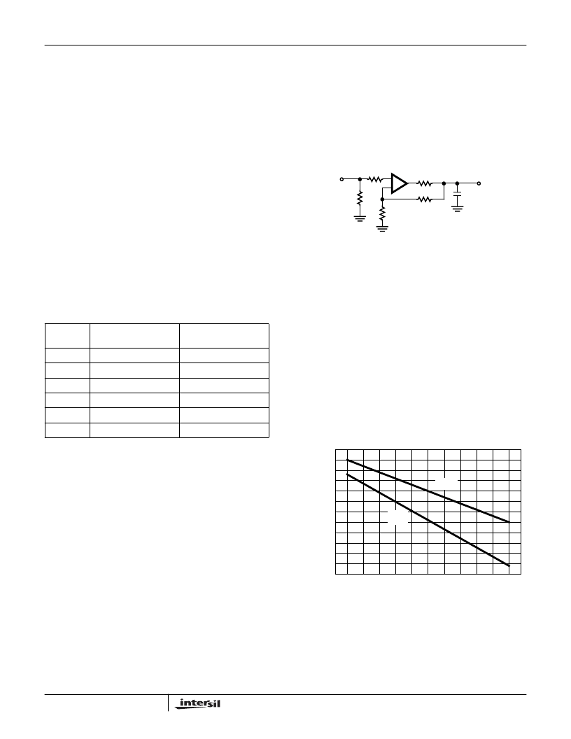
Driving Capacitive Loads
Capacitive loads will degrade the amplifier’s phase margin
resulting in frequency response peaking and possible
oscillations. In most cases the oscillation can be avoided by
placing an isolation resistor (R) in series with the output as
shown in Figure 6.
The selection criteria for the isolation resistor is highly
dependent on the load, but 27
has been determined to be
a good starting value.
Power Dissipation Considerations
Due to the high supply current inherent in quad amplifiers,
care must be taken to insure that the maximum junction
temperature (T
J
, see Absolute Maximum Ratings) is not
exceeded. Figure 7 shows the maximum ambient temperature
versus supply voltage for the available package styles (PDIP,
SOIC). At V
S
=
±
5V quiescent operation both package styles
may be operated over the full industrial range of -40
o
C to
85
o
C. It is recommended that thermal calculations, which take
into account output power, be performed by the designer.
GAIN
(A
CL
)
R
F
(
)
BANDWIDTH
(MHz)
-1
750
100
+1
1000
125
+2
681
95
+5
1000
52
+10
383
65
-10
750
22
V
IN
V
OUT
C
L
R
T
+
-
R
I
R
F
R
FIGURE 6. PLACEMENT OF THE OUTPUT ISOLATION
RESISTOR, R
100
5
7
9
11
13
15
130
120
110
100
90
80
70
60
50
40
30
20
10
SUPPLY VOLTAGE (
±
V)
PDIP
SOIC
M
o
C
FIGURE 7. MAXIMUM OPERATING AMBIENT TEMPERATURE
vs SUPPLY VOLTAGE
HA5025
相關(guān)PDF資料 |
PDF描述 |
|---|---|
| HA5025IP | Quad, 125MHz Video Current Feedback Amplifier |
| HA5025EVAL | Triple, 125MHz Video Amplifier |
| HA5135 | 2.5MHz, Precision Operational Amplifier |
| HA-5135 | 2.5MHz, Precision Operational Amplifier |
| HA-5135883 | Precision Operational Amplifier |
相關(guān)代理商/技術(shù)參數(shù) |
參數(shù)描述 |
|---|---|
| HA5025IP | 制造商:Rochester Electronics LLC 功能描述:- Bulk |
| HA503 | 制造商:未知廠家 制造商全稱:未知廠家 功能描述:Peripheral IC |
| HA-5033 | 制造商:INTERSIL 制造商全稱:Intersil Corporation 功能描述:250MHz Video Buffer |
| HA-5033_06 | 制造商:INTERSIL 制造商全稱:Intersil Corporation 功能描述:250MHz Video Buffer |
| HA5033C | 制造商:未知廠家 制造商全稱:未知廠家 功能描述:Analog IC |
發(fā)布緊急采購,3分鐘左右您將得到回復(fù)。