- 您現(xiàn)在的位置:買賣IC網(wǎng) > PDF目錄371775 > HC5513BIP (INTERSIL CORP) TVS 1500W 43V UNIDIRECT SMC PDF資料下載
參數(shù)資料
| 型號: | HC5513BIP |
| 廠商: | INTERSIL CORP |
| 元件分類: | 模擬傳輸電路 |
| 英文描述: | TVS 1500W 43V UNIDIRECT SMC |
| 中文描述: | TELECOM-SLIC, PDIP22 |
| 封裝: | PLASTIC, MS-010-AA, DIP-22 |
| 文件頁數(shù): | 12/18頁 |
| 文件大?。?/td> | 175K |
| 代理商: | HC5513BIP |

65
A filter capacitor (C
D
) in parallel with R
D
will improve the
accuracy of the trip point in a noisy environment. The value
of this capacitor is calculated using the following Equation:
Where: T = 0.5ms.
Ground Key Detector
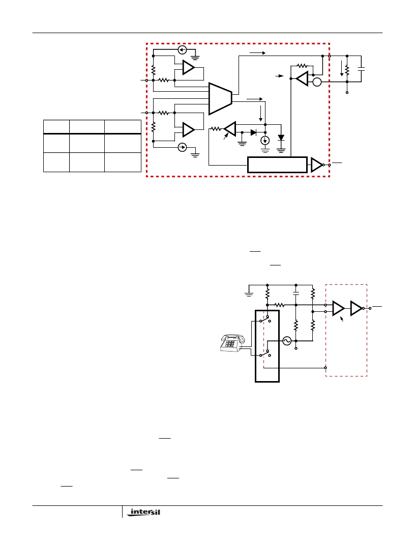
A simplified schematic of the ground key detector is shown in
Figure 18. Ground key, is the process in which the ring terminal
is shorted to ground for the purpose of signaling an Operator or
seizing a phone line (between the Central Office and a Private
Branch Exchange). The Ground Key detector is activated when
unequal current flow through resistors R1 and R2. This results
in a current (IGK) out of the transconductance amplifier (gm2)
that is equal to the product of gm2 and the differential (ITIP -
IRING) loop current. If IGK is less than the internal current
source(I1),thendiodeD1isonandtheoutputofthegroundkey
comparator is low. If IGK is greater than the internal current
source(I1),thendiodeD2isonandtheoutputofthegroundkey
comparator is high. With the output of the ground key
comparator high, and the logic configuredfor ground key detect,
the DET pin goes low. The ground key detector has a built in
hysteresis of typically 5mA between its trigger and reset values.
Ring Trip Detector
Ring trip detection is accomplished with the internal ring trip
comparator and the external circuitry shown in Figure 19. The
processofringtripisinitiatedwhenthelogicinputpinsareinthe
following states: E0 = 0, E1 = 1/0, C1 = 1 and C2 = 0. This logic
condition connects the ring trip comparator to the DET output,
and causes the Ringrly pin to energize the ring relay. The ring
relay connects the tip and ring of the phone to the external
circuitry in Figure 19. When the phone is on-hook the DT pin is
more positive than the DR pin and theDET output is high. For
off-hook conditions DR is more positive than DT andDET goes
low. When DET goes low, indicating that the phone has gone
off-hook, the SLIC is commanded by the logic inputs to go into
the active state. In the active state, tip and ring are once again
connected to the phone and normal operation ensues.
Figure 19 illustrates battery backed unbalanced ring injected
ringing. For tip injected ringing just reverse the leads to the
phone. The ringing source could also be balanced.
NOTE: The DET output will toggle at 20Hz because the DT input is
not completely filtered by C
RT
. Software can examine the duty cycle
and determine if the DET pin is low for more that half the time, if so
the off-hook condition is indicated.
Longitudinal Impedance
The feedback loop described in Figure 20(A, B) realizes the
desired longitudinal impedances from tip to ground and from
ring to ground. Nominal longitudinal impedance is resistive
and in the order of 22
.
In the presence of longitudinal currents this circuit
attenuates the voltages that would otherwise appear at the
tip and ring terminals, to levels well within the common mode
range of the SLIC. In fact, longitudinal currents may exceed
the programmed DC loop current without disturbing the
SLIC’s VF transmission capabilities.
HC5513
DET
R
D
R
2
gm
1
gm
2
gm
1
(I
METALLIC
)
R
D
C
D
V
REF
1.25V
+
-
CURRENT
LOOP
COMPARATOR
V
EE
-5V
GROUND
KEY
COMPARATOR
gm
2
(I
TIP
- I
RING
)
I
RD
R
H
I
1
D
1
D
2
I
GK
RING
TIP
+
-
R
1
+
-
CASE 1
CASE 2
CASE 3
I
METALLIC
I
LONGITUDINAL
I
LONGITUDINAL
I
METALLIC
I
LONGITUDINAL
I
LONGITUDINAL
DIGITAL MULTIPLEXER
+
-
+
-
R
H
FIGURE 18. LOOP CURRENT AND GROUND KEY DETECTORS
C
D
D
-------
=
(EQ. 27)
TIP
RING
HC5513
R
RT
V
BAT
E
RG
R
3
R
4
R
2
R
1
DR
DT
RING TRIP
COMPARATOR
DET
C
RT
RINGRLY
RING
RELAY
+
-
FIGURE 19. RING TRIP CIRCUIT FOR BATTERY BACKED RINGING
HC5513
相關(guān)PDF資料 |
PDF描述 |
|---|---|
| HC5513 | Bipolar Transistor; Package/Case:TO-220; Current Rating:7A; Voltage Rating:80V RoHS Compliant: Yes |
| HC5513BIM | TVS UNI-DIR 40V 1500W SMC |
| HC55171BIB | Low Cost 5 REN Ringing SLIC for ISDN Modem/TA and WL |
| HC55171B | Low Cost 5 REN Ringing SLIC for ISDN Modem/TA and WL |
| HC55171BIM | Low Cost 5 REN Ringing SLIC for ISDN Modem/TA and WL |
相關(guān)代理商/技術(shù)參數(shù) |
參數(shù)描述 |
|---|---|
| HC5513IMR4465 | 制造商:Rochester Electronics LLC 功能描述:- Bulk |
| HC5513IPA02 | 制造商:Harris Corporation 功能描述: |
| HC5514 | 制造商:未知廠家 制造商全稱:未知廠家 功能描述:Low Power Universal SLIC Family |
| HC55140 | 制造商:INTERSIL 制造商全稱:Intersil Corporation 功能描述:Low Power Universal SLIC Family |
| HC55140IB | 制造商:Rochester Electronics LLC 功能描述: 制造商:Intersil Corporation 功能描述: |
發(fā)布緊急采購,3分鐘左右您將得到回復(fù)。