- 您現(xiàn)在的位置:買賣IC網(wǎng) > PDF目錄384398 > HE84761 (King Billion Electronics Co., Ltd.) 8-bit Micro-controller PDF資料下載
參數(shù)資料
| 型號: | HE84761 |
| 廠商: | King Billion Electronics Co., Ltd. |
| 英文描述: | 8-bit Micro-controller |
| 中文描述: | 8位微控制器 |
| 文件頁數(shù): | 6/30頁 |
| 文件大小: | 456K |
| 代理商: | HE84761 |
第1頁第2頁第3頁第4頁第5頁當(dāng)前第6頁第7頁第8頁第9頁第10頁第11頁第12頁第13頁第14頁第15頁第16頁第17頁第18頁第19頁第20頁第21頁第22頁第23頁第24頁第25頁第26頁第27頁第28頁第29頁第30頁
King Billion Electronics Co., Ltd
駿
億
電
子
股
份
有
限
公
司
HE84761
HE80000 SERIES
August 15, 2003
This specification is subject to change without notice. Please contact sales person for the latest version before use.
Page 6 of 30
V1.2
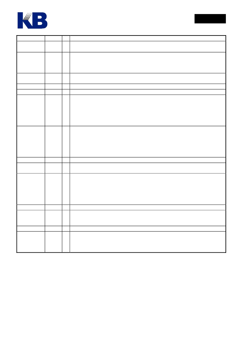
Pin Name
Pin # I/O
Description
TSTP_P
80
I
Test input pin. Please bond this pad and reserve a test point on PCB for debugging.
But for improving ESD, please connect this point with zero Ohm resistor to GND
.
External slow clock pins. Slow clock is clock source for LCD display, TIMER1,
Time-Base and other internal blocks. Both crystal and RC oscillator are provided.
The slow clock type can be selected by mask option MO_SXTAL. Choose ‘0’ for RC
type and ‘1’ for crystal oscillator.
Positive power Input. 0.1 μF decoupling capacitors should be placed as close to IC
VDD and GND pads as possible for best decoupling effect.
Power Ground Input. The TGND2 should connect with GND pin.
Power Ground Input. The TGND1 should connect with GND pin.
4-bit bi-directional I/O port 10. The output type of I/O pad can also be selected by
mask option MO_10PP[3..0] (‘1’ for push-pull and ‘0’ for open-drain).
As the output structure of I/O pad does not contain tri-state buffer. When using the
I/O pad as input pad, “1” must be outputted before reading.
PRT10[0] is shared with DTMFO of DTMF generator. PRT10[1] is multiplexed with
KEYTONE output.
8-bit bi-directional I/O port D. The output type of I/O pad can also be selected by
mask option MO_DPP[7..0] (‘1’ for push-pull and ‘0’ for open-drain).
As the output structure of I/O pad does not contain tri-state buffer. When using the
I/O as input, ‘1’ must be outputted before reading the pin.
PRTD[7..2] can be used as wake-up pins. PRTD[7..6] can be as external interrupt
sources.
O Dedicated Ground for PWM output.
The PWM output can drive speaker or buzzer directly. Set the bit2 of VOC register as
one to turn on PWM. Using VDD & PWM to drive output device.
8-bit bi-directional I/O port C. The output type of I/O pad can also be selected by
mask option MO_CPP[7..0] (‘1’ for push-pull and ‘0’ for open-drain).
As the output structure of I/O pad does not contain tri-state buffer. When using the
I/O as input, ‘1’ must be outputted before reading the pin.
PRTC[7:4] is shared with Key Scan Dedicated Input SCNI[3:0]. The Key Scan
function can be disabled by clearing MO_LCDKEY mask option to ‘0’.
P
Dedicated power input for RAM
COM[32..63] pads are shared with SEG[95..64] outputs. The functions of the pads to
be COM drivers or SEG drivers can be selected by mask option MO_COM[1..0].
Please refer to LCD driver configuration for details.
141~160 O LCD segment SEG[63..44] outputs.
LCD segments share pads with key scan out SCNO[19..0]. The key scan function of
these pins can be disabled by mask option clearing MO_LCDKEY to ‘0’, then
SGKY[43..24] function as LCD segment driver only. Setting MO_LCDKEY to ‘1’
will turn on the key scan function.
I: Input, O: Output, B: Bidirectional, P: Power.
SXO,
SXI
81,
82
O,
I
VDD
83
P
TGND2
TGND1
85
88
P
P
PRT10[3:0]
90~93
B
PRTD[7..0]
94~101 B
GND_PWM
102
PWM
103
O
PRTC[7:4]
104~107 B
VDD_RAM
108
CMSG[32..63] 109~140 O
SEG[63..44]
SGKY[43..24] 161~180 O
相關(guān)PDF資料 |
PDF描述 |
|---|---|
| HE847701 | 8-bit Micro-controller |
| HE84770D | 8-bit Micro-controller |
| HE84770 | 8-bit Micro-controller |
| HE84G752B | 8-BIT MICRO-CONTROLLER |
| HE84G761B | 8-BIT MICRO-CONTROLLER |
相關(guān)代理商/技術(shù)參數(shù) |
參數(shù)描述 |
|---|---|
| HE84761(S) | 制造商:未知廠家 制造商全稱:未知廠家 功能描述: |
| HE84762(S) | 制造商:未知廠家 制造商全稱:未知廠家 功能描述: |
| HE84770 | 制造商:KB 制造商全稱:KB 功能描述:8-bit Micro-controller |
| HE84770(S) | 制造商:未知廠家 制造商全稱:未知廠家 功能描述: |
| HE847701 | 制造商:KB 制造商全稱:KB 功能描述:8-bit Micro-controller |
發(fā)布緊急采購,3分鐘左右您將得到回復(fù)。