- 您現(xiàn)在的位置:買賣IC網(wǎng) > PDF目錄384399 > HEC4013BT (NXP Semiconductors N.V.) Dual D-type flip-flop PDF資料下載
參數(shù)資料
| 型號: | HEC4013BT |
| 廠商: | NXP Semiconductors N.V. |
| 元件分類: | 通用總線功能 |
| 英文描述: | Dual D-type flip-flop |
| 封裝: | HEC4013BT<SOT108-1 (SO14)|<<http://www.nxp.com/packages/SOT108-1.html<1<week 32, 2004,;HEC4013BT<SOT108-1 (SO14)|<<http://www.nxp.com/packages/SOT108-1.html<1<week |
| 文件頁數(shù): | 7/16頁 |
| 文件大?。?/td> | 165K |
| 代理商: | HEC4013BT |
HEF4013B
All information provided in this document is subject to legal disclaimers.
NXP B.V. 2011. All rights reserved.
Product data sheet
Rev. 7 — 13 September 2011
7 of 16
NXP Semiconductors
HEF4013B
Dual D-type flip-flop
[1]
Typical values of the propagation delays and output transition times can be calculated with the extrapolation formulas. C
L
is given in pF.
12. Waveforms
t
rec
recovery time
nSD input;
see
Figure 5
5 V
10 V
15 V
5 V
10 V
15 V
5 V
10 V
15 V
+15
15
15
40
25
25
7
14
20
5
0
0
25
10
10
14
28
40
-
-
-
-
-
-
-
-
-
ns
ns
ns
ns
ns
ns
MHz
MHz
MHz
nCD input;
see
Figure 5
f
clk(max)
maximum clock
frequency
see
Figure 4
Table 7.
T
amb
= 25
C; unless otherwise specified. For test circuit see
Figure 6
.
Symbol Parameter
Conditions
Dynamic characteristics
…continued
V
DD
Extrapolation formula Min
Typ
Max
Unit
Table 8.
V
SS
= 0 V; t
r
= t
f
20 ns; T
amb
= 25
C.
Symbol
Parameter
P
D
dynamic power dissipation
Dynamic power dissipation
V
DD
5 V P
D
= 850
f
i
+
(f
o
C
L
)
V
DD2
W
10 V P
D
= 3600
f
i
+
(f
o
C
L
)
V
DD2
W
15 V P
D
= 9000
f
i
+
(f
o
C
L
)
V
DD2
W
Typical formula
Where
f
i
= input frequency in MHz;
f
o
= output frequency in MHz;
C
L
= output load capacitance in pF;
(f
o
C
L
) = sum of the outputs;
V
DD
= supply voltage in V.
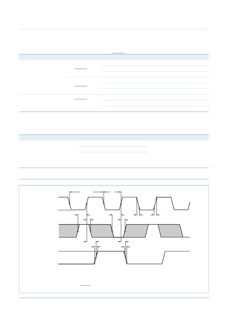
Set-up and hold times are shown as positive values but may be specified as negative values.
The shaded areas indicate when the input is permitted to change for predictable output performance.
Measurement points are given in
Table 9
.
Fig 4.
Set-up time, hold time, minimum clock pulse width, propagation delays and transition times
001aah016
0 V
0 V
t
h
t
su
1/f
clk(max)
t
h
t
su
t
f
t
r
t
W
V
M
V
M
V
M
V
I
V
OH
V
OL
V
I
output nQ
input nCP
input nD
t
t
t
t
t
PHL
t
PLH
V
Y
V
X
相關(guān)PDF資料 |
PDF描述 |
|---|---|
| HEF4013BP | Dual D-type flip-flop |
| HEF4013BT | Dual D-type flip-flop |
| HEF4014BP | 8-bit static shift register |
| HEF4014BT | 8-bit static shift register |
| HEF4015BP | Dual 4-bit static shift register |
相關(guān)代理商/技術(shù)參數(shù) |
參數(shù)描述 |
|---|---|
| HEC4013BT,112 | 功能描述:觸發(fā)器 DUAL D-TYPE RoHS:否 制造商:Texas Instruments 電路數(shù)量:2 邏輯系列:SN74 邏輯類型:D-Type Flip-Flop 極性:Inverting, Non-Inverting 輸入類型:CMOS 輸出類型: 傳播延遲時間:4.4 ns 高電平輸出電流:- 16 mA 低電平輸出電流:16 mA 電源電壓-最大:5.5 V 最大工作溫度:+ 85 C 安裝風(fēng)格:SMD/SMT 封裝 / 箱體:X2SON-8 封裝:Reel |
| HEC4013BT,118 | 功能描述:觸發(fā)器 DUAL D-TYPE RoHS:否 制造商:Texas Instruments 電路數(shù)量:2 邏輯系列:SN74 邏輯類型:D-Type Flip-Flop 極性:Inverting, Non-Inverting 輸入類型:CMOS 輸出類型: 傳播延遲時間:4.4 ns 高電平輸出電流:- 16 mA 低電平輸出電流:16 mA 電源電壓-最大:5.5 V 最大工作溫度:+ 85 C 安裝風(fēng)格:SMD/SMT 封裝 / 箱體:X2SON-8 封裝:Reel |
| HEC4013BT-T | 功能描述:觸發(fā)器 DUAL D-TYPE RoHS:否 制造商:Texas Instruments 電路數(shù)量:2 邏輯系列:SN74 邏輯類型:D-Type Flip-Flop 極性:Inverting, Non-Inverting 輸入類型:CMOS 輸出類型: 傳播延遲時間:4.4 ns 高電平輸出電流:- 16 mA 低電平輸出電流:16 mA 電源電壓-最大:5.5 V 最大工作溫度:+ 85 C 安裝風(fēng)格:SMD/SMT 封裝 / 箱體:X2SON-8 封裝:Reel |
| HEC4014 | 制造商:PHILIPS 制造商全稱:NXP Semiconductors 功能描述:8-bit static shift register |
| HEC4015 | 制造商:PHILIPS 制造商全稱:NXP Semiconductors 功能描述:Dual 4-bit static shift register |
發(fā)布緊急采購,3分鐘左右您將得到回復(fù)。