- 您現(xiàn)在的位置:買賣IC網(wǎng) > PDF目錄371806 > HFA3101B96 (INTERSIL CORP) Gilbert Cell UHF Transistor Array PDF資料下載
參數(shù)資料
| 型號(hào): | HFA3101B96 |
| 廠商: | INTERSIL CORP |
| 元件分類: | 小信號(hào)晶體管 |
| 英文描述: | Gilbert Cell UHF Transistor Array |
| 中文描述: | 6 CHANNEL, UHF BAND, Si, NPN, RF SMALL SIGNAL TRANSISTOR |
| 封裝: | SOIC-8 |
| 文件頁數(shù): | 5/12頁 |
| 文件大?。?/td> | 905K |
| 代理商: | HFA3101B96 |

3-5
Application Information
The HFA3101 array is a very versatile RF Building block. It
has been carefully laid out to improve its matching
properties, bringing the distortion due to area mismatches,
thermal distribution, betas and ohmic resistances to a
minimum.
The cell is equivalent to two differential stages built as two
“variable transconductance multipliers” in parallel, with their
outputs cross coupled. This configuration is well known in
the industry as a Gilbert Cell which enables a four quadrant
multiplication operation.
Due to the input dynamic range restrictions for the input
levels at the upper quad transistors and lower tail transistors,
the HFA3101 cell has restricted use as a linear four quadrant
multiplier. However, its configuration is well suited for uses
where its linear response is limited to one of the inputs only,
as in modulators or mixer circuit applications. Examples of
these circuits are up converters, down converters, frequency
doublers and frequency/phase detectors.
Although linearization is still an issue for the lower pair input,
emitter degeneration can be used to improve the dynamic
range and consequent linearity. The HFA3101 has the lower
pair emitters brought to external pins for this purpose.
In modulators applications, the upper quad transistors are
used in a switching mode where the pairs Q
1
/Q
2
and Q
3
/Q
4
act as non saturating high speed switches. These switches
are controlled by the signal often referred as the carrier
input. The signal driving the lower pair Q
5
/Q
6
is commonly
used as the modulating input. This signal can be linearly
transferred to the output by either the use of low signal levels
(Well below the thermal voltage of 26mV) or by the use of
emitter degeneration. The chopped waveform appearing at
the output of the upper pair (Q
1
to Q
4
) resembles a signal
that is multiplied by +1 or -1 at every half cycle of the
switching waveform.
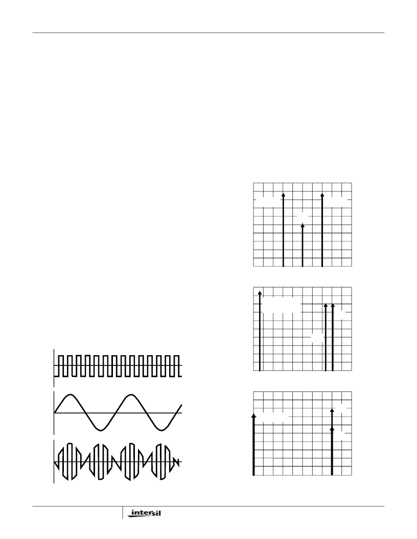
Figure 1 shows the typical input waveforms where the
frequency of the carrier is higher than the modulating signal.
The output waveform shows a typical suppressed carrier
output of an up converter or an AM signal generator.
Carrier suppression capability is a property of the well known
Balanced modulator in which the output must be zero when
one or the other input (carrier or modulating signal) is equal
to zero. however, at very high frequencies, high frequency
mismatches and AC offsets are always present and the
suppression capability is often degraded causing carrier and
modulating feedthrough to be present.
Being a frequency translation circuit, the balanced modulator
has the properties of translating the modulating frequency
(
ω
M
) to the carrier frequency (
ω
C
), generating the two side
bands
ω
U
=
ω
C
+
ω
M
and
ω
L
= ω
C
-
ω
M
. Figure 2 shows
some translating schemes being used by
balanced mixers.
CARRIER SIGNAL
MODULATING SIGNAL
DIFFERENTIAL OUTPUT
+1
-1
FIGURE 1. TYPICAL MODULATOR SIGNALS
FIGURE 2A. UP CONVERSION OR SUPPRESSED CARRIER AM
FIGURE 2B. DOWN CONVERSION
FIGURE 2C. ZERO IF OR DIRECT DOWN CONVERSION
FIGURE 2. MODULATOR FREQUENCY SPECTRUM
ω
C
+
ω
M
ω
C
-
ω
M
ω
C
IF
(
ω
C
-
ω
M
)
FOLDED BACK
ω
M
ω
C
BASEBAND
ω
C
ω
M
HFA3101
相關(guān)PDF資料 |
PDF描述 |
|---|---|
| HFA3101BZ | Gilbert Cell UHF Transistor Array |
| HFA3101 | Gilbert Cell UHF Transistor Array(Gb 單元超高頻晶體管陣列) |
| HFA3101BZ96 | Gilbert Cell UHF Transistor Array |
| HFA3134IH96 | Ultra High Frequency Matched Pair Transistors |
| HFA3134 | Ultra High Frequency Matched Pair Transistors |
相關(guān)代理商/技術(shù)參數(shù) |
參數(shù)描述 |
|---|---|
| HFA3101BZ | 功能描述:射頻雙極小信號(hào)晶體管 TXARRAY NPN GILBERT CELL 8W RoHS:否 制造商:NXP Semiconductors 配置:Single 晶體管極性:NPN 最大工作頻率:7000 MHz 集電極—發(fā)射極最大電壓 VCEO:15 V 發(fā)射極 - 基極電壓 VEBO:2 V 集電極連續(xù)電流:0.15 A 功率耗散:1000 mW 直流集電極/Base Gain hfe Min: 最大工作溫度:+ 150 C 封裝 / 箱體:SOT-223 封裝:Reel |
| HFA3101BZ | 制造商:Intersil Corporation 功能描述:TRANSISTOR ARRAY |
| HFA3101BZ | 制造商:Intersil Corporation 功能描述:IC TRANSISTOR ARRAY GILBERT 制造商:Intersil Corporation 功能描述:IC TRANSISTOR ARRAY, GILBERT |
| HFA3101BZ96 | 功能描述:射頻雙極小信號(hào)晶體管 TXARRAY NPN GILBERT CELL 8W MILEL RoHS:否 制造商:NXP Semiconductors 配置:Single 晶體管極性:NPN 最大工作頻率:7000 MHz 集電極—發(fā)射極最大電壓 VCEO:15 V 發(fā)射極 - 基極電壓 VEBO:2 V 集電極連續(xù)電流:0.15 A 功率耗散:1000 mW 直流集電極/Base Gain hfe Min: 最大工作溫度:+ 150 C 封裝 / 箱體:SOT-223 封裝:Reel |
| HFA3102 | 制造商:INTERSIL 制造商全稱:Intersil Corporation 功能描述:Dual Long-Tailed Pair Transistor Array |
發(fā)布緊急采購,3分鐘左右您將得到回復(fù)。