- 您現(xiàn)在的位置:買賣IC網(wǎng) > PDF目錄371822 > HIP7038A8F (HARRIS SEMICONDUCTOR) J1850 8-Bit 68HC05 Microcontroller 8K EEPROM Version PDF資料下載
參數(shù)資料
| 型號: | HIP7038A8F |
| 廠商: | HARRIS SEMICONDUCTOR |
| 元件分類: | 微控制器/微處理器 |
| 英文描述: | J1850 8-Bit 68HC05 Microcontroller 8K EEPROM Version |
| 中文描述: | 8-BIT, EEPROM, 10 MHz, MICROCONTROLLER, CDSO28 |
| 文件頁數(shù): | 3/5頁 |
| 文件大?。?/td> | 21K |
| 代理商: | HIP7038A8F |
9-101
Specifications HIP7038A8
Absolute Maximum Ratings
Thermal Information
Operating Temperature Range (T
A
) . . . . . . . . . . . .-40
o
C to +125
o
C
Storage Temperature Range (T
STG
) . . . . . . . . . . . .-65
o
C to +150
o
C
Junction Temperature . . . . . . . . . . . . . . . . . . . . . . . . . . . . . . +150
o
C
Lead Temperature (During Soldering) . . . . . . . . . . . . . . . . +265
o
C
1/16in.
±
1/32in. (1.59
±
0.79mm) from case for 10s Max.
Supply Voltage (V
DD
) . . . . . . . . . . . . . . . . . . . . . . . . . -0.3V to +6.0V
Input or Output Voltage
Pins with V
DD
Diode . . . . . . . . . . . . . . . . . . . . -0.3V to V
DD
+0.3V
Pins without V
DD
Diode. . . . . . . . . . . . . . . . . . . . . -0.3V to +10.0V
Current Drain Per Pin, I (Excluding V
DD
and V
SS
) . . . . . . . . 25mA
ESD Classification . . . . . . . . . . . . . . . . . . . . . . . . . . . . . . . . Class 2
Gate Count. . . . . . . . . . . . . . . . . . . . . . . . . . . . . . . . . . 21000 Gates
CAUTION: Stresses above those listed in “Absolute Maximum Ratings” may cause permanent damage to the device. This is a stress only rating and operation
of the device at these or any other conditions above those indicated in the operational sections of this specification is not implied.
Operating Conditions
Operating Voltage Range. . . . . . . . . . . . . . . . . . . . . +4.5V to +5.5V
Operating Temperature Range. . . . . . . . . . . . . . . . . -40
o
C to +85
o
C
Input Low Voltage. . . . . . . . . . . . . . . . . . . . . . . . . . . . . . 0V to +0.8V
Input High Voltage. . . . . . . . . . . . . . . . . . . . . . . . . .(0.8V
DD
) to V
DD
Input Rise and Fall Time
CMOS Inputs. . . . . . . . . . . . . . . . . . . . . . . . . . . . . . . .100ns Max.
CMOS Schmitt Inputs . . . . . . . . . . . . . . . . . . . . . . . . . . .Unlimited
DC Electrical Specifications
V
DD
= 5V
DC
±
10%, V
SS
= 0V
DC
, T
A
= -40
o
C to +85
o
C Unless Otherwise Specified.
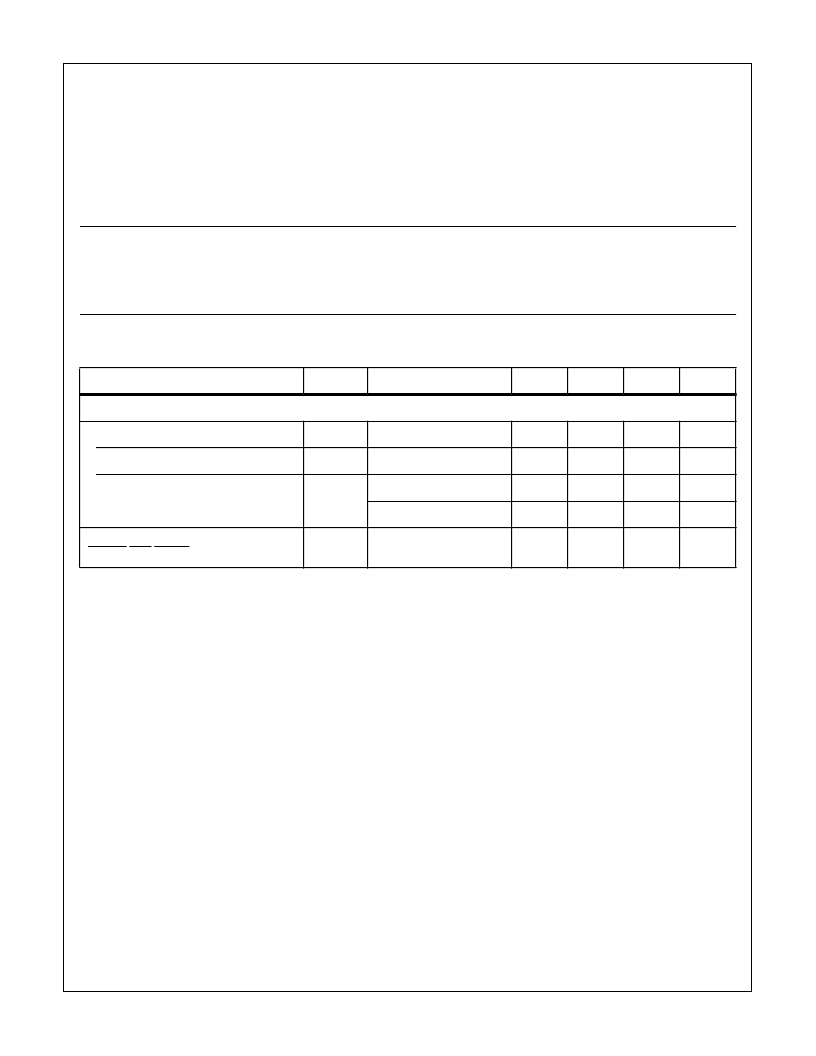
PARAMETERS
SYMBOL
CONDITIONS
MIN
TYP
MAX
UNITS
SUPPLY CURRENT
RUN
I
RUN
-
50
-
mA
WAIT
I
WAIT
-
4
-
mA
STOP
I
STOP
T
A
= +25
o
C
-
100
-
μ
A
T
A
= -40
o
C to +85
o
C
-
100
-
μ
A
Powerdown Input Voltage:
RESET, IRQ, VPWIN, OSCIN
V
INPD
V
DD
= 0
-0.3
-
9
V
NOTE:
1. This device contains circuitry to protect the inputs against damage due to high static voltages of electric fields; however, it is advised that
normal precautions be taken to avoid application of any voltage higher than maximum rated voltages to this high impedance circuit. For
proper operation it is recommended that V
IN
and V
OUT
be constrained to the range V
SS
<(V
IN
or V
OUT
)<V
DD
. Reliability of operation is
enhanced if unused inputs except OSC2 are connected to an appropriate logic voltage level (e.g., either V
SS
or V
DD
).
相關PDF資料 |
PDF描述 |
|---|---|
| HIP7038A8 | J1850 8-Bit 68HC05 Microcontroller 8K EEPROM Version |
| HJF-A-200 | Analog IC |
| HJF-A-300 | Analog IC |
| HJK-0505S | DC-to-DC Voltage Converter |
| HJK-0512D | DC-to-DC Voltage Converter |
相關代理商/技術參數(shù) |
參數(shù)描述 |
|---|---|
| HIP8112A | 制造商:HARRIS 制造商全稱:HARRIS 功能描述:NTSC/PAL Video Decoder |
| HIP-8V | 制造商:Belden Inc 功能描述:SPLITTER 8 WAY |
| HIP9010 | 制造商:INTERSIL 制造商全稱:Intersil Corporation 功能描述:Engine Knock Signal Processor |
| HIP9010AB | 制造商:Intersil Corporation 功能描述: |
| HIP9011 | 制造商:INTERSIL 制造商全稱:Intersil Corporation 功能描述:Engine Knock Signal Processor |
發(fā)布緊急采購,3分鐘左右您將得到回復。