- 您現(xiàn)在的位置:買賣IC網(wǎng) > PDF目錄385383 > HIRF840 (HSMC CORP.) N-Channel Power MOSFET PDF資料下載
參數(shù)資料
| 型號(hào): | HIRF840 |
| 廠商: | HSMC CORP. |
| 英文描述: | N-Channel Power MOSFET |
| 中文描述: | N溝道功率MOSFET |
| 文件頁(yè)數(shù): | 2/4頁(yè) |
| 文件大小: | 47K |
| 代理商: | HIRF840 |
HI-SINCERITY
MICROELECTRONICS CORP.
Spec. No. : MOS200505
Issued Date : 2005.06.01
Revised Date : 2005.06.08
Page No. : 2/4
HIRF840, HIRF840F
HSMC Product Specification
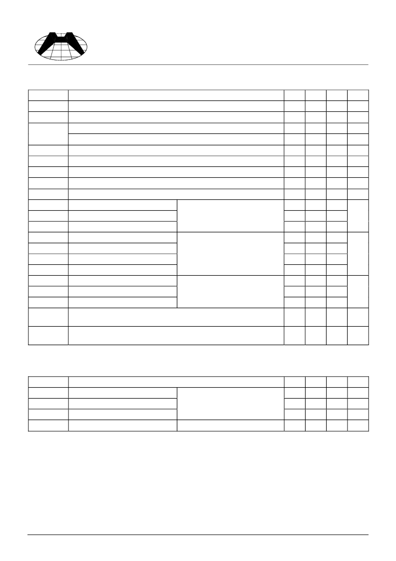
ELectrical Characteristics
(T
j
=25
°
C, unless otherwise specified)
Symbol
V
(BR)DSS
V
(BR)DSS
/
T
J
Breakdown Voltage Temp. Coefficient (Reference to 25
o
C, I
D
=1mA)
Drain-Source Leakage Current (V
DS
=500V, V
GS
=0V)
I
DSS
Drain-Source Leakage Current (V
DS
=400V, V
GS
=0V, T
j
=125
°
C)
I
GSSF
Gate-Source Leakage Current-Forward (V
gsf
=20V, V
DS
=0V)
I
GSSR
Gate-Source Leakage Current-Reverse (V
gsr
=-20V, V
DS
=0V)
V
GS(th)
Gate Threshold Voltage (V
DS
=V
GS
, I
D
=250uA)
R
DS(on)
Static Drain-Source On-Resistance (V
GS
=10V, I
D
=4.8A)(*4)
g
FS
Forward Transconductance (V
DS
=50V, I
D
=4.8A)(*4)
C
iss
Input Capacitance
C
oss
Output Capacitance
C
rss
Reverse Transfer Capacitance
t
d(on)
Turn-on Delay Time
t
r
Rise Time
t
d(off)
Turn-off Delay Time
t
f
Fall Time
Q
g
Total Gate Charge
Q
gs
Gate-Source Charge
Q
gd
Gate-Drain Charge
Internal Drain Inductance (Measured from the drain lead 0.25” from
package to center of die)
Internal Source Inductance (Measured from the drain lead 0.25” from
package to source bond pad)
Characteristic
Min.
500
-
Typ.
-
0.78
Max.
-
-
Unit
V
V/
o
C
Drain-Source Breakdown Voltage (V
GS
=0V, I
D
=250uA)
-
-
25
250
uA
uA
-
-
2
-
-
-
-
-
100
-100
4
0.85
nA
nA
V
S
4.9
-
-
-
-
-
-
-
-
-
-
-
-
-
-
-
-
-
-
-
1300
310
120
14
23
49
20
-
-
-
V
DS
=25V, V
GS
=0V, f=1MHz
pF
(V
DD
=250V, I
D
=8A, R
G
=9.1
,
R
D
=31
)(*4)
ns
63
9.3
32
(V
DS
=400V, I
D
=8A, V
GS
=10V)
(*4)
nC
L
D
-
4.5
-
nH
L
S
-
7.5
-
nH
*4: Pulse Test: Pulse Width
≤
300us, Duty Cycle
≤
2%
Source-Drain Diode
Symbol
Q
rr
t
on
t
rr
V
SD
Characteristic
Min.
-
-
-
Typ.
4.2
**
460
Max.
8.9
-
970
Units
uC
Reverse Recovery Charge
Forward Turn-On Time
Reverse Recovery Time
I
F
=8A, d
i
/d
t
=100A/us, T
j
=25
°
C (*4)
ns
Diode Forward Voltage
I
S
=8A, V
GS
=0V, T
j
=25
°
C (*4)
-
-
2
V
**: Negligible, Dominated by circuit inductance
相關(guān)PDF資料 |
PDF描述 |
|---|---|
| HIRF840F | N-Channel Power MOSFET |
| HJK-20VH | Frequency Mixer |
| HK-2900 | Differential Positive ECL (DPECL) |
| HK-A2910-FREQ | Frequency Range: 100.0 MHz to 320.0 MHz |
| HK-A2911-FREQ | Frequency Range: 100.0 MHz to 320.0 MHz |
相關(guān)代理商/技術(shù)參數(shù) |
參數(shù)描述 |
|---|---|
| HIRF840F | 制造商:HSMC 制造商全稱:HSMC 功能描述:N-Channel Power MOSFET |
| HIRHR10A-7R-5SB(73) | 制造商:Hirose 功能描述: |
| HIRK-315 | 制造商:RFSOLUTIONS 制造商全稱:rfsolutions.ltd 功能描述:RF RECEIVER DECODER HYBRID |
| HIRK-315A | 制造商:RFSOLUTIONS 制造商全稱:rfsolutions.ltd 功能描述:RF RECEIVER DECODER HYBRID |
| HIRK-433 | 制造商:RFSOLUTIONS 制造商全稱:rfsolutions.ltd 功能描述:RF RECEIVER DECODER HYBRID |
發(fā)布緊急采購(gòu),3分鐘左右您將得到回復(fù)。