- 您現(xiàn)在的位置:買(mǎi)賣(mài)IC網(wǎng) > PDF目錄60836 > HMC261LM1 (HITTITE MICROWAVE CORP) 20000 MHz - 32000 MHz RF/MICROWAVE WIDE BAND LOW POWER AMPLIFIER PDF資料下載
參數(shù)資料
| 型號(hào): | HMC261LM1 |
| 廠商: | HITTITE MICROWAVE CORP |
| 元件分類(lèi): | 放大器 |
| 英文描述: | 20000 MHz - 32000 MHz RF/MICROWAVE WIDE BAND LOW POWER AMPLIFIER |
| 封裝: | PLASTIC, SMT, 8 PIN |
| 文件頁(yè)數(shù): | 7/8頁(yè) |
| 文件大小: | 466K |
| 代理商: | HMC261LM1 |
MICROWAVE CORPORATION
1 - 14
For price, delivery, and to place orders, please contact Hittite Microwave Corporation:
12 Elizabeth Drive, Chelmsford, MA 01824 Phone: 978-250-3343 Fax: 978-250-3373
Visit us at www.hittite.com, or Email at sales@hittite.com
AMPLIFIERS
-
SMT
1
HMC261LM1
SMT DISTRIBUTED GaAs
MMIC AMPLIFIER, 20 - 32 GHz
v03.1201
Preparation & Handling of the LM1 Millimeterwave Package for Surface Mounting
HMC261LM1 Recommended SMT Attachment Technique
The HMC LM1 package was designed to be compatible with
high volume surface mount PCB assembly processes. The
LM1 package requires a specic mounting pattern to allow
proper mechanical attachment and to optimize electrical per-
formance at millimeterwave frequencies. The PCB layout pat-
tern can be found on each LM1 product data sheet. It can also
be provided as an electronic drawing upon request from Hittite
Sales & Application Engineering.
Follow these precautions to avoid permanent damage:
Cleanliness: Observe proper handling procedures to ensure
clean devices and PCBs. LM1 devices should remain in their
original packaging until component placement to ensure no
contamination or damage to RF, DC & ground contact areas.
Static Sensitivity: Follow ESD precautions to protect against
ESD strikes.
General Handling: Handle the LM1 package on the top with a vacuum collet or along the edges with a sharp pair of
bent tweezers. Avoid damaging the RF, DC, & ground contacts on the package bottom. Do not apply excess pres-
sure to the top of the lid.
Solder Materials & Temperature Prole: Follow the information contained in the application note. Hand soldering is
not recommended. Conductive epoxy attachment is not recommended.
Solder Paste
Solder paste should be selected based on the user’s experience and should be compatible with the metallization
systems used. See the LM1 data sheet Outline drawing for pin & ground contact metallization schemes.
Solder Paste Application
Solder paste is generally applied to the PCB using either a stencil printer or dot placement. The volume of solder
paste will be dependent on PCB and component layout and should be controlled to ensure consistent mechanical &
electrical performance. Excess solder may create unwanted electrical parasitics at high frequencies.
Solder Reow
The soldering process is usually accomplished in a reow oven but may also use a vapor phase process. A solder
reow prole is suggested above.
Prior to reowing product, temperature proles should be measured using the same mass as the actual assemblies.
The thermocouple should be moved to various positions on the board to account for edge and corner effects and
varying component masses. The nal prole should be determined by mounting the thermocouple to the PCB at the
location of the device.
Follow solder paste and oven vendor’s recommendations when developing a solder reow prole. A standard prole
will have a steady ramp up from room temperature to the pre-heat temperature to avoid damage due to thermal
shock. Allow enough time between reaching pre-heat temperature and reow for the solvent in the paste to evaporate
and the ux to completely activate. Reow must then occur prior to the ux being completely driven off. The duration
of peak reow temperature should not exceed 15 seconds. Packages have been qualied to withstand a peak
temperature of 2350C for 15 seconds. Verify that the prole will not expose the device to temperatures in excess of
2350C.
Cleaning
A water-based ux wash may be used.
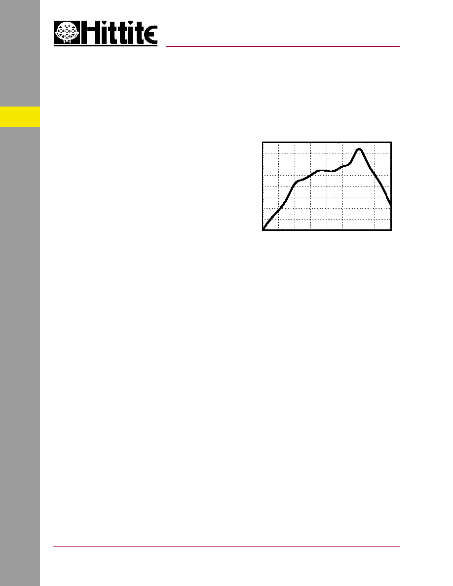
25
50
75
100
125
150
175
200
225
01
23
45
67
8
TEMPERATURE
(
0 C)
TIME (min)
Recommended solder reflow profile
for HMC LM1 SMT package
DISCONTINUED
PRODUCT
Not
Recommended
for New
Designs
相關(guān)PDF資料 |
PDF描述 |
|---|---|
| HMC263 | 24000 MHz - 36000 MHz RF/MICROWAVE WIDE BAND LOW POWER AMPLIFIER |
| HMC264 | 20000 MHz - 32000 MHz RF/MICROWAVE DOUBLE BALANCED MIXER, 13 dB CONVERSION LOSS-MAX |
| HMC265LM3 | RF/MICROWAVE DOWN CONVERTER |
| HMC267QS16G | RF/MICROWAVE MODULATOR |
| HMC271ALP4E | 700 MHz - 3700 MHz RF/MICROWAVE VARIABLE ATTENUATOR, 3.3 dB INSERTION LOSS-MAX |
相關(guān)代理商/技術(shù)參數(shù) |
參數(shù)描述 |
|---|---|
| HMC261LM1_01 | 制造商:HITTITE 制造商全稱(chēng):Hittite Microwave Corporation 功能描述:SMT DISTRIBUTED GaAs MMIC AMPLIFIER, 20 - 32 GHz |
| HMC262 | 制造商:HITTITE 制造商全稱(chēng):Hittite Microwave Corporation 功能描述:GaAs MMIC LOW NOISE AMPLIFIER 15 - 24 GHz |
| HMC262_00 | 制造商:HITTITE 制造商全稱(chēng):Hittite Microwave Corporation 功能描述:GaAs MMIC LOW NOISE AMPLIFIER, 15 - 24 GHz |
| HMC262_02 | 制造商:HITTITE 制造商全稱(chēng):Hittite Microwave Corporation 功能描述:GaAs MMIC LOW NOISE AMPLIFIER, 15 - 24 GHz |
| HMC263 | 制造商:HITTITE 制造商全稱(chēng):Hittite Microwave Corporation 功能描述:GaAs MMIC LOW NOISE AMPLIFIER, 24 - 36 GHz |
發(fā)布緊急采購(gòu),3分鐘左右您將得到回復(fù)。