- 您現(xiàn)在的位置:買賣IC網(wǎng) > PDF目錄60851 > HMMC-5021 2000 MHz - 22000 MHz RF/MICROWAVE WIDE BAND LOW POWER AMPLIFIER PDF資料下載
參數(shù)資料
| 型號: | HMMC-5021 |
| 元件分類: | 放大器 |
| 英文描述: | 2000 MHz - 22000 MHz RF/MICROWAVE WIDE BAND LOW POWER AMPLIFIER |
| 封裝: | 0.1173 X 0.0303 INCH, DIE |
| 文件頁數(shù): | 3/6頁 |
| 文件大小: | 113K |
| 代理商: | HMMC-5021 |
3
Applications
The HMMC-5021/26 series of
traveling wave amplifiers are
designed for use as general
purpose wideband gain blocks in
commu-nication systems and
microwave instrumentation. They
are ideally suited for broadband
applications requiring a flat gain
re-sponse and excellent port
matches over a 2 to 26.5 GHz
frequency range. Dynamic gain
control and low-frequency
extension capabilities are de-
signed into these devices.
Biasing and Operation
These amplifiers are biased with
a single positive drain supply
(V
DD) and a single negative gate
supply (V
G1). The recommended
bias conditions for the
HMMC-5021/26 are V
DD = 7.0 V,
I
DD = 150 mA for best overall
performance. To achieve this
drain current level, V
G1 is typi-
cally biased between -0.2V and -
0.5V. No other bias supplies or
connections to the device are
required for 2 to 26.5 GHz
operation. See Figure 3 for
assembly information.
The HMMC-5021/26 is a DC
coupled amplifier. External cou-
pling capacitors are needed on
RF IN and RF OUT ports. The
drain bias pad is connected to RF
and must be decoupled to the
lowest operating frequency.
The auxiliary gate and drain con-
tacts are provided when perfor-
mance below 1 GHz in required.
Connect external capacitors to
ground to maintain input and
output VSWR at low frequencies
(see Additional References). Do
not apply bias to these pads.
The second gate (V
G2 ) can be
used to obtain 35 dB (typical)
dynamic gain control. For normal
operation, no external bias is
required on this contact and its
self-bias voltage is
≈ +2.1V.
Applying an external bias be-
tween its open-circuit voltage
and -2.5 volts will adjust the gain
while maintaining a good input/
output port match.
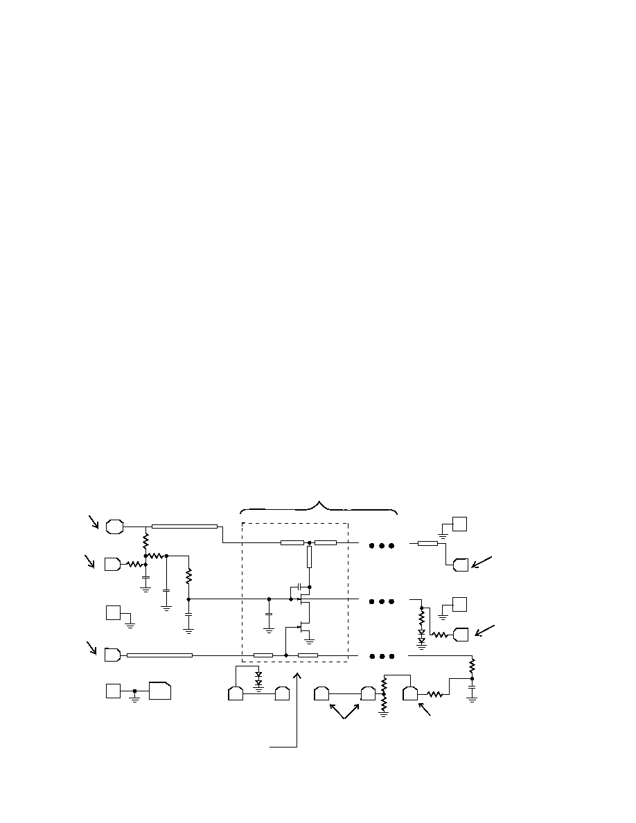
Aux. Drain
Drain Bias
(VDD)
RF Input
Single Stage Shown
Temp
Diode
Sense
Temp
Diode
Force
First Gate
Bias (VG1)
Second Gate
Bias (VG2)
RF Output
Aux. Gate
Note:
FET gate periphery in microns.
Seven Identical Stages
124
Figure 1. Schematic.
Assembly Techniques
GaAs MMICs are ESD sensitive.
ESD preventive measures must be
employed in all aspects of storage,
handling, and assembly. MMIC
ESD precautions, handling consid-
erations, die attach and bonding
methods are critical factors in
successful GaAs MMIC perfor-
mance and reliability. Avago
application note #54, “GaAs MMIC
ESD, Die Attach and Bonding
Guidelines” provides basic infor-
mation on these subjects.
Additional References
AN# 31, “2–26.5 GHz Variable Gain
Amplifier Using HMMC-5021/22/26
and HMMC-1002 GaAs MMIC,”
AN# 34, “HMMC-5021/22/26/27
TWA Environmental Data,” AN# 41,
“HMMC-5021/22/26 S-Parameters
Performance as a Function of
Bonding Configuration,” AN# 47,
“HMMC-5021/22/26 2–26.5 GHz
GaAs MMIC Distributed Amplifier
Conversion Guide,” and AN# 1053,
“Designing with HMMC-5021/22/26
and HMMC-5027 GaAs MMIC
Amplifiers.”
相關PDF資料 |
PDF描述 |
|---|---|
| HMMC-5026 | 2000 MHz - 26500 MHz RF/MICROWAVE WIDE BAND LOW POWER AMPLIFIER |
| HMMC-5023 | 21200 MHz - 26500 MHz RF/MICROWAVE WIDE BAND LOW POWER AMPLIFIER |
| HMMC-5025 | 2000 MHz - 50000 MHz RF/MICROWAVE WIDE BAND LOW POWER AMPLIFIER |
| HMMC-5025 | 2000 MHz - 50000 MHz RF/MICROWAVE WIDE BAND LOW POWER AMPLIFIER |
| HMMC-5026 | 2000 MHz - 26500 MHz RF/MICROWAVE WIDE BAND LOW POWER AMPLIFIER |
相關代理商/技術參數(shù) |
參數(shù)描述 |
|---|---|
| HMMC-5022 | 制造商:Agilent Technologies 功能描述:RF AMP MOD SGL GP AMP 22GHZ 8V CHIP - Gel-pak, waffle pack, wafer, diced wafer on film 制造商:Agilent Technologies 功能描述:ML-GAAS ATTEN CHIP |
| HMMC-5023 | 制造商:Agilent Technologies 功能描述:RF AMP MOD SGL GP AMP 26.5GHZ 7V - Gel-pak, waffle pack, wafer, diced wafer on film |
| HMMC-5025 | 制造商:Agilent Technologies 功能描述:RF AMP MOD SGL GP AMP 50GHZ 7V - Gel-pak, waffle pack, wafer, diced wafer on film |
| HMMC-5026 | 制造商:Agilent Technologies 功能描述:RF AMP MOD SGL GP AMP 26.5GHZ 8V - Gel-pak, waffle pack, wafer, diced wafer on film |
| HMMC-5027 | 制造商:Agilent Technologies 功能描述:RF AMP MOD SGL PWR AMP 26.5GHZ 8V CHIP - Gel-pak, waffle pack, wafer, diced wafer on film |
發(fā)布緊急采購,3分鐘左右您將得到回復。