- 您現(xiàn)在的位置:買賣IC網(wǎng) > PDF目錄296194 > HPC46400EV2 (National Semiconductor Corporation) High-Performance Communications MicroController PDF資料下載
參數(shù)資料
| 型號: | HPC46400EV2 |
| 廠商: | National Semiconductor Corporation |
| 英文描述: | High-Performance Communications MicroController |
| 中文描述: | 高性能通信微控制器 |
| 文件頁數(shù): | 7/30頁 |
| 文件大小: | 362K |
| 代理商: | HPC46400EV2 |
第1頁第2頁第3頁第4頁第5頁第6頁當(dāng)前第7頁第8頁第9頁第10頁第11頁第12頁第13頁第14頁第15頁第16頁第17頁第18頁第19頁第20頁第21頁第22頁第23頁第24頁第25頁第26頁第27頁第28頁第29頁第30頁
Timer Overview (Continued)
The timers T1 through T3 in conjunction with their registers
form Timer-Register pairs The registers hold the pulse du-
ration values All the Timer-Register pairs can be read from
or written to Each timer can be started or stopped under
software control Once enabled the timers count down and
upon underflow the contents of its associated register are
automatically loaded into the timer
SYNCHRONOUS OUTPUTS
The flexible timer structure of the HPC46400E simplifies
pulse generation and measurement There are four syn-
chronous timer outputs (TS0 through TS3) that work in con-
junction with the timer T2 The synchronous timer outputs
can be used either as regular outputs or individually pro-
grammed to toggle on timer T2 underflows (see
Figure 12 )
Maximum output frequency for any timer output can be ob-
tained by setting timerregister pair to zero This then will
produce an output frequency equal to
the frequency of
the source used for clocking the timer
Timer Registers
There are four control registers that program the timers The
divide by (DIVBY) register programs the clock input to tim-
ers T2 and T3 The timer mode register (TMMODE) contains
control bits to start and stop timers T1 through T3 It also
contains bits to latch acknowledge and enable interrupts
from timers T0 through T3
Timer Applications
The use of Pulse Width Timers for the generation of various
waveforms is easily accomplished by the HPC46400E
Frequencies can be generated by using the timerregister
pairs A square wave is generated when the register value is
a constant The duty cycle can be controlled simply by
changing the register value
TLDD10422 – 22
FIGURE 13 Square Wave Frequency Generation
Synchronous outputs based on Timer T2 can be generated
on the 4 outputs TS0 – TS3 Each output can be individually
programmed to toggle on T2 underflow Register R2 con-
tains the time delay between events
Figure 14 is an exam-
ple of synchronous pulse train generation
TLDD10422 – 23
FIGURE 14 Synchronous Pulse Generation
WATCHDOG Logic
The WATCHDOG Logic monitors the operations taking
place and signals upon the occurrence of any illegal activity
The illegal conditions that trigger the WATCHDOG logic are
potentially infinite loops Should the WATCHDOG register
not be written to before Timer T0 overflows twice or more
often than once every 4096 counts an infinite loop condi-
tion is assumed to have occurred The illegal condition
forces the Watch Out (WO) pin low The WO pin is an open
drain output and can be connected to the RESET or NMI
inputs or to the users external logic
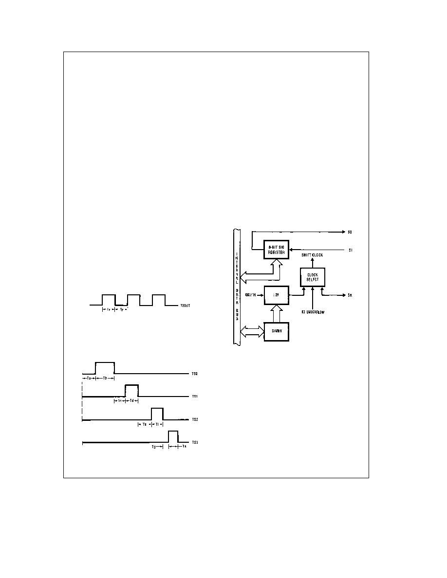
MICROWIREPLUS
MICROWIREPLUS is used for synchronous serial data
communications (see
Figure 15 ) MICROWIREPLUS has
an 8-bit parallel-loaded serial shift register using SI as the
input and SO as the output SK is the clock for the serial
shift register (SIO) The SK clock signal can be provided by
an internal or external source The internal clock rate is pro-
grammable by the DIVBY register A DONE flag indicates
when the data shift is completed
The MICROWIREPLUS capability enables it to interface
with any of National Semiconductor’s MICROWIRE periph-
erals (ie ISDN Transceivers AD converters display driv-
ers EEPROMs)
TLDD10422 – 24
FIGURE 15 MICROWIREPLUS
15
相關(guān)PDF資料 |
PDF描述 |
|---|---|
| HPH-12/30-D48PBHL2-C | 1-OUTPUT 360 W DC-DC REG PWR SUPPLY MODULE |
| HPSTP-19-5000-01 | INTERCONNECTION DEVICE |
| HPT-136-01-SM-D-RA | 72 CONTACT(S), MALE, RIGHT ANGLE TWO PART BOARD CONNECTOR, SOLDER |
| HPT-153-01-L-D-RA | 106 CONTACT(S), MALE, RIGHT ANGLE TWO PART BOARD CONNECTOR, SOLDER |
| HPT-153-01-LM-D-RA | 106 CONTACT(S), MALE, RIGHT ANGLE TWO PART BOARD CONNECTOR, SOLDER |
相關(guān)代理商/技術(shù)參數(shù) |
參數(shù)描述 |
|---|---|
| HPC46400EV20 | 功能描述:16位微控制器 - MCU RoHS:否 制造商:Texas Instruments 核心:RISC 處理器系列:MSP430FR572x 數(shù)據(jù)總線寬度:16 bit 最大時鐘頻率:24 MHz 程序存儲器大小:8 KB 數(shù)據(jù) RAM 大小:1 KB 片上 ADC:Yes 工作電源電壓:2 V to 3.6 V 工作溫度范圍:- 40 C to + 85 C 封裝 / 箱體:VQFN-40 安裝風(fēng)格:SMD/SMT |
| HPC46400EV20/NOPB | 功能描述:16位微控制器 - MCU RoHS:否 制造商:Texas Instruments 核心:RISC 處理器系列:MSP430FR572x 數(shù)據(jù)總線寬度:16 bit 最大時鐘頻率:24 MHz 程序存儲器大小:8 KB 數(shù)據(jù) RAM 大小:1 KB 片上 ADC:Yes 工作電源電壓:2 V to 3.6 V 工作溫度范圍:- 40 C to + 85 C 封裝 / 箱體:VQFN-40 安裝風(fēng)格:SMD/SMT |
| HPC46400EVHG2 | 制造商:NSC 制造商全稱:National Semiconductor 功能描述:High-Performance Communications MicroController |
| HPC46400EVHG20 | 制造商:NSC 制造商全稱:National Semiconductor 功能描述:High-Performance Communications MicroController |
| HPC46400L20 | 制造商:未知廠家 制造商全稱:未知廠家 功能描述:16-Bit Microcontroller |
發(fā)布緊急采購,3分鐘左右您將得到回復(fù)。