- 您現(xiàn)在的位置:買賣IC網(wǎng) > PDF目錄370699 > HSMS-282E Surface Mount RF Schottky Barrier Diodes(表貼型射頻肖特基勢壘二極管) PDF資料下載
參數(shù)資料
| 型號: | HSMS-282E |
| 英文描述: | Surface Mount RF Schottky Barrier Diodes(表貼型射頻肖特基勢壘二極管) |
| 中文描述: | 表面貼裝射頻肖特基二極管(表貼型射頻肖特基勢壘二極管) |
| 文件頁數(shù): | 6/12頁 |
| 文件大小: | 141K |
| 代理商: | HSMS-282E |

6
R
S
is seen in a curve that droops
at high current). All Schottky
diode curves have the same slope,
but not necessarily the same
value of current for a given
voltage. This is determined by the
saturation current, I
S
, and is
related to the barrier height of the
diode.
Through the choice of p-type or
n-type silicon, and the selection
of metal, one can tailor the
characteristics of a Schottky
diode. Barrier height will be
altered, and at the same time C
J
and R
S
will be changed. In
general, very low barrier height
diodes (with high values of I
S
,
suitable for zero bias applica-
tions) are realized on p-type
silicon. Such diodes suffer from
higher values of R
S
than do the
n-type. Thus, p-type diodes are
generally reserved for detector
applications (where very high
values of R
V
swamp out high R
S
)
and n-type diodes such as the
HSMS-282x are used for mixer
applications (where high L.O.
drive levels keep R
V
low). DC
biased detectors and self-biased
detectors used in gain or power
control circuits.
Detector Applications
Detector circuits can be divided
into two types, large signal
(P
in
> -20 dBm) and small signal
(P
in
< -20 dBm). In general, the
former use resistive impedance
matching at the input to improve
flatness over frequency—this is
possible since the input signal
levels are high enough to produce
adequate output voltages without
the need for a high Q reactive
input matching network. These
circuits are self-biased (no
external DC bias) and are used
for gain and power control of
amplifiers.
Small signal detectors are used as
very low cost receivers, and
require a reactive input imped-
ance matching network to
achieve adequate sensitivity and
output voltage. Those operating
with zero bias utilize the HSMS-
285x family of detector diodes.
However, superior performance
over temperature can be achieved
with the use of 3 to 30
μ
A of DC
bias. Such circuits will use the
HSMS-282x family of diodes if the
operating frequency is 1.5 GHz or
lower.
Typical performance of single
diode detectors (using
HSMS-2820 or HSMS-282B) can
be seen in the transfer curves
given in Figures 7 and 8. Such
detectors can be realized either
as series or shunt circuits, as
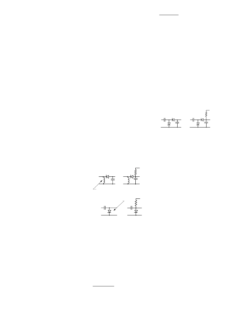
shown in Figure 11.
DC Bias
Shunt inductor provides
video signal return
Shunt diode provides
video signal return
DC Bias
DC Biased Diodes
Zero Biased Diodes
Figure 11. Single Diode Detectors.
The series and shunt circuits can
be combined into a voltage
doubler
[1]
, as shown in Figure 12.
The doubler offers three advan-
tages over the single diode
circuit.
The two diodes are in parallel
in the RF circuit, lowering the
input impedance and making
the design of the RF matching
network easier.
The two diodes are in series
in the output (video) circuit,
doubling the output voltage.
Some cancellation of
even-order harmonics takes
place at the input.
DC Bias
DC Biased Diodes
Zero Biased Diodes
Figure 12. Voltage Doubler.
The most compact and lowest
cost form of the doubler is
achieved when the HSMS-2822 or
HSMS-282C series pair is used.
Both the detection sensitivity and
the DC forward voltage of a
biased Schottky detector are
temperature sensitive. Where
both must be compensated over a
wide range of temperatures, the
differential detector
[2]
is often
used. Such a circuit requires that
the detector diode and the
reference diode exhibit identical
characteristics at all DC bias
levels and at all temperatures.
This is accomplished through the
use of two diodes in one package,
for example the HSMS-2825 in
Figure 13. In the Agilent assembly
facility, the two dice in a surface
mount package are taken from
adjacent sites on the wafer (as
illustrated in Figure 14). This
[1]
Agilent Application Note 956-4, “Schottky Diode Voltage Doubler.”
[2]
Raymond W. Waugh, “Designing Large-Signal Detectors for Handsets and Base
Stations,”
Wireless Systems Design,
Vol. 2, No. 7, July 1997, pp 42 – 48.
相關(guān)PDF資料 |
PDF描述 |
|---|---|
| HSMS-282F | Surface Mount RF Schottky Barrier Diodes(表貼型射頻肖特基勢壘二極管) |
| HSMS-282K | Surface Mount RF Schottky Barrier Diodes(表貼型射頻肖特基勢壘二極管) |
| HSMS-282L | Surface Mount RF Schottky Barrier Diodes(表貼型射頻肖特基勢壘二極管) |
| HSMS-282M | Surface Mount RF Schottky Barrier Diodes(表貼型射頻肖特基勢壘二極管) |
| HSMS-282N | Surface Mount RF Schottky Barrier Diodes(表貼型射頻肖特基勢壘二極管) |
相關(guān)代理商/技術(shù)參數(shù) |
參數(shù)描述 |
|---|---|
| HSMS-282E-BLK | 制造商:AGILENT 制造商全稱:AGILENT 功能描述:Surface Mount RF Schottky Barrier Diodes |
| HSMS-282E-BLKG | 功能描述:肖特基二極管與整流器 15 VBR 1 pF RoHS:否 制造商:Skyworks Solutions, Inc. 產(chǎn)品:Schottky Diodes 峰值反向電壓:2 V 正向連續(xù)電流:50 mA 最大浪涌電流: 配置:Crossover Quad 恢復(fù)時間: 正向電壓下降:370 mV 最大反向漏泄電流: 最大功率耗散:75 mW 工作溫度范圍:- 65 C to + 150 C 安裝風格:SMD/SMT 封裝 / 箱體:SOT-143 封裝:Reel |
| HSMS-282E-TR1 | 制造商:AGILENT 制造商全稱:AGILENT 功能描述:Surface Mount RF Schottky Barrier Diodes |
| HSMS-282E-TR1G | 功能描述:肖特基二極管與整流器 15 VBR 1 pF RoHS:否 制造商:Skyworks Solutions, Inc. 產(chǎn)品:Schottky Diodes 峰值反向電壓:2 V 正向連續(xù)電流:50 mA 最大浪涌電流: 配置:Crossover Quad 恢復(fù)時間: 正向電壓下降:370 mV 最大反向漏泄電流: 最大功率耗散:75 mW 工作溫度范圍:- 65 C to + 150 C 安裝風格:SMD/SMT 封裝 / 箱體:SOT-143 封裝:Reel |
| HSMS-282E-TR2 | 制造商:AGILENT 制造商全稱:AGILENT 功能描述:Surface Mount RF Schottky Barrier Diodes |
發(fā)布緊急采購,3分鐘左右您將得到回復(fù)。