- 您現(xiàn)在的位置:買賣IC網(wǎng) > PDF目錄383075 > HSP50214BVC (HARRIS SEMICONDUCTOR) Programmable Downconverter PDF資料下載
參數(shù)資料
| 型號(hào): | HSP50214BVC |
| 廠商: | HARRIS SEMICONDUCTOR |
| 元件分類: | 通信及網(wǎng)絡(luò) |
| 英文描述: | Programmable Downconverter |
| 中文描述: | SPECIALTY TELECOM CIRCUIT, PQFP120 |
| 文件頁(yè)數(shù): | 42/60頁(yè) |
| 文件大小: | 573K |
| 代理商: | HSP50214BVC |
第1頁(yè)第2頁(yè)第3頁(yè)第4頁(yè)第5頁(yè)第6頁(yè)第7頁(yè)第8頁(yè)第9頁(yè)第10頁(yè)第11頁(yè)第12頁(yè)第13頁(yè)第14頁(yè)第15頁(yè)第16頁(yè)第17頁(yè)第18頁(yè)第19頁(yè)第20頁(yè)第21頁(yè)第22頁(yè)第23頁(yè)第24頁(yè)第25頁(yè)第26頁(yè)第27頁(yè)第28頁(yè)第29頁(yè)第30頁(yè)第31頁(yè)第32頁(yè)第33頁(yè)第34頁(yè)第35頁(yè)第36頁(yè)第37頁(yè)第38頁(yè)第39頁(yè)第40頁(yè)第41頁(yè)當(dāng)前第42頁(yè)第43頁(yè)第44頁(yè)第45頁(yè)第46頁(yè)第47頁(yè)第48頁(yè)第49頁(yè)第50頁(yè)第51頁(yè)第52頁(yè)第53頁(yè)第54頁(yè)第55頁(yè)第56頁(yè)第57頁(yè)第58頁(yè)第59頁(yè)第60頁(yè)
3-42
The PDC begins to fill the buffer each time an interval
number of samples have passed. The number of sample
sets the PDC writes into the buffer and is programmed into
bits 3-0 of Control Word 21. The number of samples stored
is the programmed value and may be from 1 to 8 sample
sets. A sample set consists of I, Q, |r|,
φ
and
.
In snap shot operations, the buffer is read the same as for
FIFO operations. Figures 37 and 39 describe the Design
Blocks and Timing required to output data on AOUT(7:0) and
BOUT(7:0). Table 17 summarizes the selectable output
signals. The method for reading data through the
Microprocessor Section in snap shot mode is identical to the
method described in the FIFO mode subsection and the
Microprocessor Read Section.
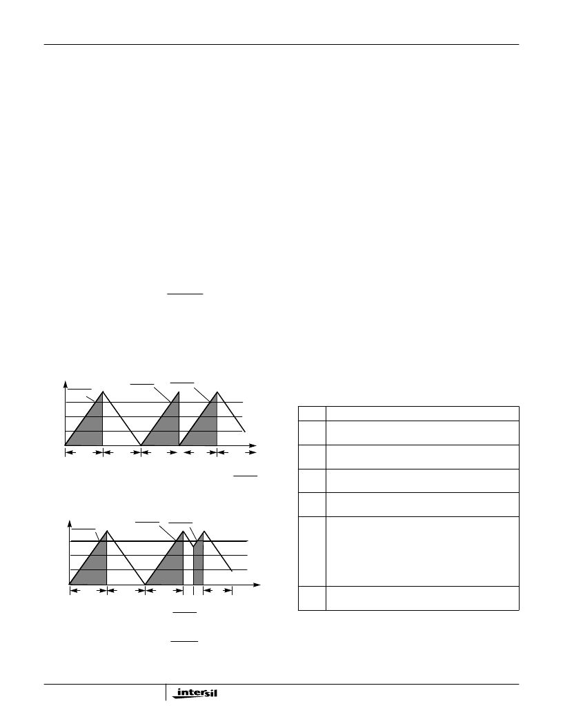
Avoiding Timing Pitfalls When Using the Buffer
RAM Output Port
In snapshot mode, the whole buffer is written whenever the
interval counter has timed-out. After time-out, old data can
be written over. Thus, the data contained within the buffer
must be retrieved before time-out to avoid data loss.
It may be desirable to disable the INTRRPT into the
controlling microprocessor during read cycles to avoid the
generating extra interrupts. Figure 44 details how the WRITE
address can trigger extra interrupts. Care must be taken to
either read sufficient data out of memory or RESET the
addressing to ensure that a complete set of data is the
cause of the interrupt.
Microprocessor Write Section
The Microprocessor Write Section uses an indirect
addressing scheme where a 32-bit data word is first loaded in
a four 8-bit byte master registers using four writes via C(7:0).
The desired destination register address is then written to
another address using C(7:0). Writing this address triggers a
circuit that generates a pulse, synchronous to clock, that loads
the Destination Register. The sync circuits and data words are
synchronized to different clocks, CLKIN or PROCCLK,
depending on the Destination Registers.
A(2:0) determines the destination for the data on bus, C(7:0).
Table 19 shows the address map for microprocessor interface.
Figure 45 shows the Control Register loading sequence. The
data in C(7:0) and address map in A(2:0) is loaded into the
PDC on the rising edge of WR and is latched into the Master
Register on the rising edge of WR and A(2:0) = 100. Four
clocks must pass before loading the next Control Word to
guarantee that the data has been transferred.
Some registers can be loaded (i.e., transferred from the
Master Register to a Configuration Register or from a Holding
Register to an active register) by initiating a sync. For
example, to load the AGC Gain, the value of the AGC gain is
first loaded into the Holding Registers, then a transfer is
initiated by SYNCIN2 if Control Word 8, Bit 29 = 1. This allows
the AGC gain to be loaded by detecting a system event, such
as a start of a new burst. Bit 20 of Control Word 0 has the
same effect on the Carrier NCO center frequency for
assertion of SYNCIN1, except it transfers from a dedicated
holding register - not the Master Register.
Suppose a (0018D038)H needs to be loaded into Control Word
0, then Table 20 details the steps to be taken.
TIME
A
WR
RD
WR
R
WR
RD
W
A: NORMAL READ/WRITE SEQUENCE
TIME
A
W
RD
W
R
B: FALSE TRIGGERED INTERRUPT READ/WRITE SEQUENCE
INTRRP
INTRRP
INTRRP
INTRRP
INTRRP
INTRRP
A COMPLETE SET OF 3 DATA SAMPLES IS IN MEMORY AT INTRRP
THE THIRD INTERRUPT HAS ONLY 1 NEW DATA ENTRY
(INSTEAD OF 3) AT INTRRP
FIGURE 44. AVOIDING FALSE INTRRP ASSERTIONS
WR
RD
WR
TABLE 19. DEFINITION OF ADDRESS MAP
A2-0
REGISTER DESCRIPTION
0
Holding Register 0. Transfers to bits 7-0 of the 32-bit Des-
tination Register. Bit 0 is the LSB of the 32-bit register.
1
Holding Register 1. Transfers to bits 15-8 of a 32-bit Desti-
nation Register.
2
Holding Register 2. Transfers to bits 23-16 of a 32-bit Des-
tination Register.
3
Holding Register 3. Transfers to bits 31-24 of a 32-bit Des-
tination Register. Bit 31 is the MSB of the 32-bit register.
4
This is the Destination Address Register. On the fourth
CLK following a write to this register, the contents of the
Holding Registers are transferred to the Destination Reg-
ister. All 8 bits written to this register are decoded into the
Destination Register Address. The configuration destina-
tion address map is given in the tables in the Control Word
Section.
5
Selects data source for reading. See Microprocessor Read
Section.
HSP50214B
相關(guān)PDF資料 |
PDF描述 |
|---|---|
| HSP50214BVI | Programmable Downconverter |
| HT84 | ADSL Coupling Transformers |
| HT84-00594 | ADSL Coupling Transformers |
| HT8400594S | ADSL Coupling Transformers |
| HT84-00595 | ADSL Coupling Transformers |
相關(guān)代理商/技術(shù)參數(shù) |
參數(shù)描述 |
|---|---|
| HSP50214BVCZ | 功能描述:上下轉(zhuǎn)換器 120L MQFP COMTEMP 14-BIT PROG DWNCNVRT RoHS:否 制造商:Texas Instruments 產(chǎn)品:Down Converters 射頻:52 MHz to 78 MHz 中頻:300 MHz LO頻率: 功率增益: P1dB: 工作電源電壓:1.8 V, 3.3 V 工作電源電流:120 mA 最大功率耗散:1 W 最大工作溫度:+ 85 C 安裝風(fēng)格:SMD/SMT 封裝 / 箱體:PQFP-128 |
| HSP50214BVI | 功能描述:上下轉(zhuǎn)換器 120L MQFP INDTEMP 14-BIT PROGRAMMABLE DOWNCONVERTER 65MSPS RoHS:否 制造商:Texas Instruments 產(chǎn)品:Down Converters 射頻:52 MHz to 78 MHz 中頻:300 MHz LO頻率: 功率增益: P1dB: 工作電源電壓:1.8 V, 3.3 V 工作電源電流:120 mA 最大功率耗散:1 W 最大工作溫度:+ 85 C 安裝風(fēng)格:SMD/SMT 封裝 / 箱體:PQFP-128 |
| HSP50214BVIZ | 功能描述:上下轉(zhuǎn)換器 120L MQFP INDTEMP 14-BIT PROG DWNCNVRT RoHS:否 制造商:Texas Instruments 產(chǎn)品:Down Converters 射頻:52 MHz to 78 MHz 中頻:300 MHz LO頻率: 功率增益: P1dB: 工作電源電壓:1.8 V, 3.3 V 工作電源電流:120 mA 最大功率耗散:1 W 最大工作溫度:+ 85 C 安裝風(fēng)格:SMD/SMT 封裝 / 箱體:PQFP-128 |
| HSP50214VC | 制造商:Rochester Electronics LLC 功能描述:- Bulk |
| HSP50214VI | 制造商:Rochester Electronics LLC 功能描述:- Bulk |
發(fā)布緊急采購(gòu),3分鐘左右您將得到回復(fù)。