- 您現(xiàn)在的位置:買賣IC網(wǎng) > PDF目錄370725 > HV2405E (Harris Corporation) World-Wide Single Chip Power Supply PDF資料下載
參數(shù)資料
| 型號: | HV2405E |
| 廠商: | Harris Corporation |
| 英文描述: | World-Wide Single Chip Power Supply |
| 中文描述: | 環(huán)球單片電源 |
| 文件頁數(shù): | 8/14頁 |
| 文件大?。?/td> | 573K |
| 代理商: | HV2405E |

5-22
HV-2405E
Setting The Output Voltage
The circuits shown in Figure 7 and Figure 8 provide a regu-
lated 5V to 24V
DC
output voltage that is set by adjusting the
value of Z1. The output voltage of the HV-2405E (pin 6) is
set by feedback to the sense pin (pin 5). The output will rise
to the voltage necessary to keep the sense pin at 5V. The
output voltage is equal to the Zener voltage (V
Z1
) plus the 5V
on the sense pin. For a 5V output, pin 5 and pin 6 would be
shorted together. The output voltage has the accuracy and
tolerance of both the Zener diode and the band-gap of the
HV-2405E (see Figure 16). The maximum output voltage is
limited by Z
B2
to
≈
34V
DC
. Z
B2
protects the output by ensur-
ing that an overvoltage condition does not exist. Note: the
output voltage can also be set by placing a resistor (1/4W)
between pin 5 and pin 6. If a resistor is placed between pin 5
and pin 6 an additional 1V per k
(
±
10%) is added to the 5V
output.
Optimizing Design
(Imbedded Supply)
Selecting the storage capacitor C2
For applications requiring less than 30mA, the value of C2
can be reduced for a more cost effective solution. The mini-
mum C2 capacitor value vs. output current is presented in
Table 2. Advantages of making C2 as small as possible are:
Reduced total size and cost of the circuit.
Reduced start up time.
Consideration should be given to the tolerance and tempera-
ture coefficient of the C2 value selected. (Note: momentary
peak output current demands should be considered in the
sizing of C2. Increasing the output capacitor C4 is another
way to supply momentary peak current demands.)
TABLE 2. IMBEDDED SUPPLY
R1 - 150
R2 = 2.7
V
IN
FREQ.
50Hz
C2
I
OUT
30mA
24mA
14mA
8mA
30mA
27mA
16mA
9mA
30mA
30mA
16mA
8mA
30mA
30mA
16mA
9mA
264Vrms
330
μ
F
220
μ
F
100
μ
F
50
μ
F
330
μ
F
220
μ
F
100
μ
F
50
μ
F
330
μ
F
220
μ
F
100
μ
F
50
μ
F
330
μ
F
220
μ
F
100
μ
F
50
μ
F
264Vrms
60Hz
132Vrms
50Hz
132Vrms
60Hz
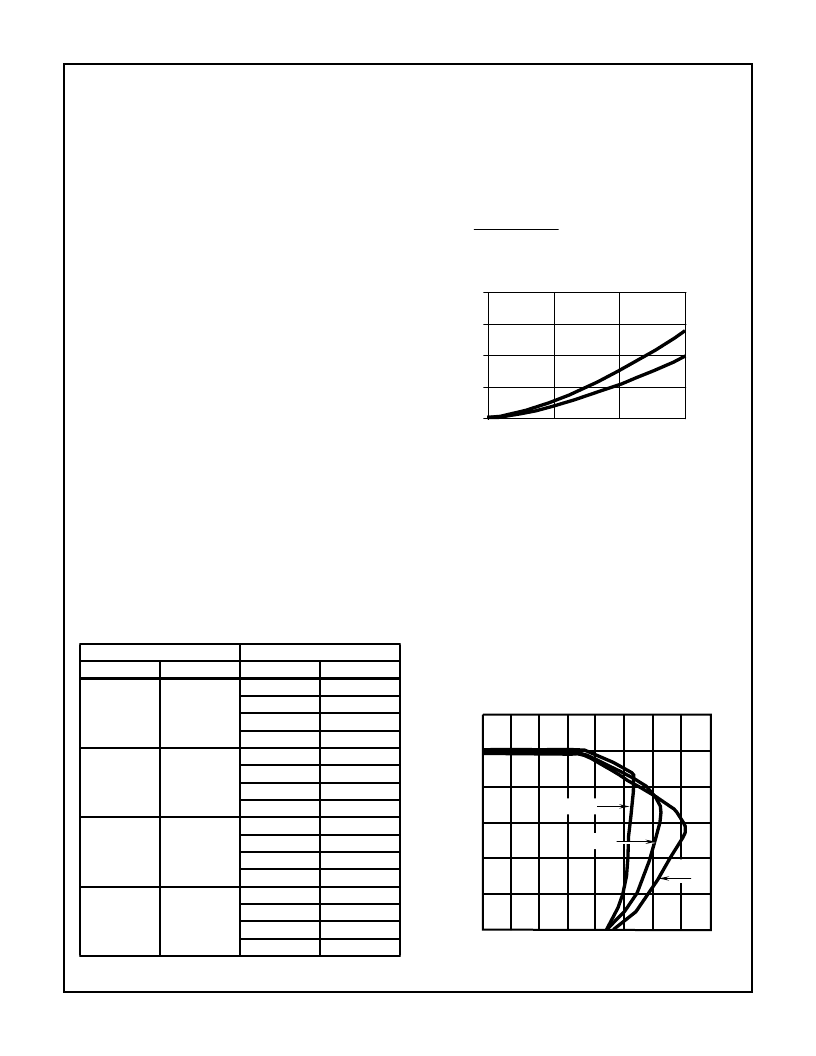
Determining the Power Dissipation in R1
Circuit efficiency is limited by the power dissipation in R1.
The power dissipation for 240Vrms and 120Vrms is shown in
Figure 11.
For input voltages other than 240Vrms or 120Vrms Equation
10 can be used to determine the power dissipation in R1.
FIGURE 11. POWER DISSIPATION IN R1 vs LOAD CURRENT
Operation information
Effects of Temperature on Output Current
Figure 12 and Figure 13 show the effects of temperature on
the output current for the imbedded supply (R2 = 2.7
).
Fig-
ure 12 illustrates V
OUT
= 5V operation and Figure 13 illus-
trates V
OUT
= 24V operation. The imbedded supply (R2 =
2.7
)
delivers 30mA output current across the specified tem-
perature range of -40
o
C to +85
o
C for all output voltages
between 5V and 24V. The effect of decreasing the value of
C2 (330
μ
F) reduces the maximum output current (i.e. moves
curve to the left). For all C2 values selected from Table 2
(assuming tolerance and temperature coefficient are taken
into account) the circuit meets the expected output current
across the above mentioned temperature range.
FIGURE 12. OUTPUT CURRENT vs TEMPERATURE (R1 = 150
,
Pd = 2.8
(EQ. 10)
√
R1 Vrms (I
OUT
)
3
LOAD CURRENT (mA)
P
0
1
2
3
4
0
10
20
30
120Vrms
240Vrms
IMBEDDED SUPPLY (R1 = 150
)
5
4
3
2
1
0
0
10
20
OUTPUT CURRENT (mA)
30
40
50
60
70
80
O
6
+85
o
C
-40
o
C
+25
o
C
IMBEDDED SUPPLY
Application Information
(Continued)
相關(guān)PDF資料 |
PDF描述 |
|---|---|
| HV3-2405E-5 | World-Wide Single Chip Power Supply |
| HV3-2405E-9 | World-Wide Single Chip Power Supply |
| HV3-2405E-5 | PT 21C 21#16 SKT PLUG |
| HV3-2405E-9 | World-WideSingle Chip Power Supply |
| HV341C | Interface IC |
相關(guān)代理商/技術(shù)參數(shù) |
參數(shù)描述 |
|---|---|
| HV-2405E | 制造商:HARRIS 制造商全稱:HARRIS 功能描述:World-Wide Single Chip Power Supply |
| HV250 | 制造商:TESTEC 功能描述:PROBE HIGH VOLTAGE 2.5KV 制造商:TESTEC 功能描述:PROBE, HIGH VOLTAGE, 2.5KV 制造商:TESTEC 功能描述:PROBE, HIGH VOLTAGE, 2.5KV; Test Probe Type:Various; Test Probe Functions:Voltage; For Use With:Oscilloscopes; SVHC:No SVHC (19-Dec-2012); Attenuation:x100; Bandwidth:300MHz; External Length / Height:1.2m; Input Impedance:100Mohm; |
| HV250A | 功能描述:氣體放電管 - GDT /氣體等離子體避雷器 2500V RoHS:否 制造商:Bourns 峰值脈沖電流: 直流擊穿電壓(標(biāo)稱):4500 V 電極數(shù)量:2 系列:SA2 端接類型:Axial 故障安全保護(hù) Y/N: 封裝:Reel |
| HV250C | 功能描述:氣體放電管 - GDT /氣體等離子體避雷器 2500V RoHS:否 制造商:Bourns 峰值脈沖電流: 直流擊穿電壓(標(biāo)稱):4500 V 電極數(shù)量:2 系列:SA2 端接類型:Axial 故障安全保護(hù) Y/N: 封裝:Reel |
| HV2512AA1008F100S2 | 制造商:VISHAY 制造商全稱:Vishay Siliconix 功能描述:High Voltage Chip Resistors |
發(fā)布緊急采購,3分鐘左右您將得到回復(fù)。