- 您現(xiàn)在的位置:買賣IC網(wǎng) > PDF目錄385414 > HY29F002TT-70 (HYNIX SEMICONDUCTOR INC) 2 Megabit (256K x 8), 5 Volt-only, Flash Memory PDF資料下載
參數(shù)資料
| 型號(hào): | HY29F002TT-70 |
| 廠商: | HYNIX SEMICONDUCTOR INC |
| 元件分類: | DRAM |
| 英文描述: | 2 Megabit (256K x 8), 5 Volt-only, Flash Memory |
| 中文描述: | 256K X 8 FLASH 5V PROM, 70 ns, PDSO32 |
| 封裝: | TSOP-32 |
| 文件頁數(shù): | 2/38頁 |
| 文件大?。?/td> | 381K |
| 代理商: | HY29F002TT-70 |
第1頁當(dāng)前第2頁第3頁第4頁第5頁第6頁第7頁第8頁第9頁第10頁第11頁第12頁第13頁第14頁第15頁第16頁第17頁第18頁第19頁第20頁第21頁第22頁第23頁第24頁第25頁第26頁第27頁第28頁第29頁第30頁第31頁第32頁第33頁第34頁第35頁第36頁第37頁第38頁
2
Rev. 4.1/May 01
HY29F002T
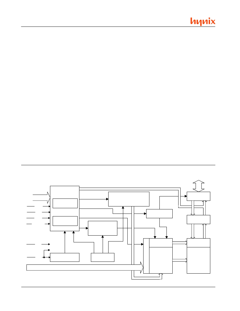
BLOCK DIAGRAM
STATE
CONTROL
WE#
CE#
OE#
COMMAND
REGISTER
DQ[7:0]
V
CC
DETECTOR
TIMER
ERASE VOLTAGE
GENERATOR AND
SECTOR SWITCHES
PROGRAM
VOLTAGE
GENERATOR
A
X-DECODER
Y-DECODER
2 MBIT
FLASH
MEMORY
ARRAY
(7 Sectors)
Y-GATING
DATA LATCH
I/O BUFFERS
I/O CONTROL
DQ[7:0]
A[17:0]
ELECTRONIC
ID
V
CC
V
SS
RESET#
HY29F002T has separate chip enable (CE#), write
enable (WE#) and output enable (OE#) controls.
The device is compatible with the JEDEC single
power-supply Flash command set standard. Com-
mands are written to the command register using
standard microprocessor write timings, from where
they are routed to an internal state-machine that
controls the erase and programming circuits.
Device programming is performed a byte at a time
by executing the four-cycle Program Command.
This initiates an internal algorithm that automati-
cally times the program pulse widths and verifies
proper cell margin.
The HY29F002T
’
s sector erase architecture allows
any number of array sectors to be erased and re-
programmed without affecting the data contents
of other sectors. Device erasure is initiated by
executing the Erase Command. This initiates an
internal algorithm that automatically preprograms
the array (if it is not already programmed) before
executing the erase operation. During erase
cycles, the device automatically times the erase
pulse widths and verifies proper cell margin.
To protect data in the device from accidental or
unauthorized attempts to program or erase the
device while it is in the system (e.g., by a virus),
the device has a Sector Protect function which
hardware write protects selected sectors. The
sector protect and unprotect features can be en-
abled in a PROM programmer. Temporary Sec-
tor Unprotect, which requires a high voltage, al-
lows in-system erasure and code changes in pre-
viously protected sectors.
Erase Suspend enables the user to put erase on
hold for any period of time to read data from, or
program data to, any sector that is not selected
for erasure. True background erase can thus be
achieved. The device is fully erased when shipped
from the factory.
Addresses and data needed for the programming
and erase operations are internally latched during
write cycles, and the host system can detect
completion of a program or erase operation by
reading the DQ[7] (Data# Polling) and DQ[6]
(toggle) status bits. Reading data from the device
is similar to reading from SRAM or EPROM de-
vices. Hardware data protection measures include
a low V
CC
detector that automatically inhibits write
operations during power transitions.
The host can place the device into the standby
mode. Power consumption is greatly reduced in
this mode.
相關(guān)PDF資料 |
PDF描述 |
|---|---|
| HY29F002TT-90 | 2 Megabit (256K x 8), 5 Volt-only, Flash Memory |
| HY29F040A | 512K x 8-bit CMOS 5.0 volt-only, Sector Erase Flash Memory |
| HY29F080T70 | 8 Megabit (1M x 8), 5 Volt-only, Flash Memory |
| HY29F080 | 8 Megabit (1M x 8), 5 Volt-only, Flash Memory |
| HY29F080G12 | 8 Megabit (1M x 8), 5 Volt-only, Flash Memory |
相關(guān)代理商/技術(shù)參數(shù) |
參數(shù)描述 |
|---|---|
| HY29F002TT-70E | 制造商:未知廠家 制造商全稱:未知廠家 功能描述:x8 Flash EEPROM |
| HY29F002TT-70I | 制造商:未知廠家 制造商全稱:未知廠家 功能描述:x8 Flash EEPROM |
| HY29F002TT-90 | 制造商:HYNIX 制造商全稱:Hynix Semiconductor 功能描述:2 Megabit (256K x 8), 5 Volt-only, Flash Memory |
| HY29F002TT-90E | 制造商:未知廠家 制造商全稱:未知廠家 功能描述:x8 Flash EEPROM |
| HY29F002TT-90I | 制造商:未知廠家 制造商全稱:未知廠家 功能描述:x8 Flash EEPROM |
發(fā)布緊急采購,3分鐘左右您將得到回復(fù)。