- 您現(xiàn)在的位置:買賣IC網(wǎng) > PDF目錄385414 > HY29F080G-90 (HYNIX SEMICONDUCTOR INC) x8 Flash EEPROM PDF資料下載
參數(shù)資料
| 型號: | HY29F080G-90 |
| 廠商: | HYNIX SEMICONDUCTOR INC |
| 元件分類: | DRAM |
| 英文描述: | x8 Flash EEPROM |
| 中文描述: | 1M X 8 FLASH 5V PROM, 90 ns, PDSO44 |
| 封裝: | PLASTIC, SOP-44 |
| 文件頁數(shù): | 5/38頁 |
| 文件大?。?/td> | 366K |
| 代理商: | HY29F080G-90 |
第1頁第2頁第3頁第4頁當(dāng)前第5頁第6頁第7頁第8頁第9頁第10頁第11頁第12頁第13頁第14頁第15頁第16頁第17頁第18頁第19頁第20頁第21頁第22頁第23頁第24頁第25頁第26頁第27頁第28頁第29頁第30頁第31頁第32頁第33頁第34頁第35頁第36頁第37頁第38頁
5
Rev. 6.1/May 01
HY29F080
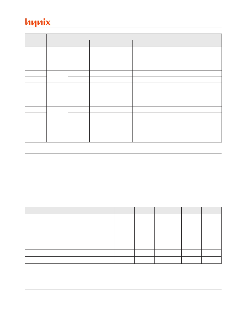
Table 1. HY29F080 Memory Array Organization
r
o
t
e
S
r
o
u
t
e
S
r
G
p
o
s
s
e
r
d
d
A
]
1
0
0
1
1
0
0
1
1
0
0
1
1
0
0
1
1
p
[
u
A
o
r
G
r
o
t
e
S
1
[
A
0
0
0
0
1
1
1
1
0
0
0
0
1
1
1
1
/
o
t
e
S
]
1
0
0
0
0
0
0
0
0
1
1
1
1
1
1
1
1
1
]
:
1
[
A
e
g
n
a
R
s
s
e
r
d
d
A
[
A
]
]
1
0
1
0
1
0
1
0
1
0
1
0
1
0
1
0
1
[
A
0
1
2
3
4
5
6
7
8
9
0
1
1
S
1
S
1
S
1
S
1
S
S
S
S
S
S
S
S
S
S
S
S
0
G
S
F
F
F
F
F
F
F
F
F
F
F
F
F
F
F
F
F
F
F
F
F
F
F
F
F
F
F
F
F
F
F
F
F
F
F
F
F
F
F
F
F
F
F
F
F
F
F
F
F
F
F
F
F
F
F
F
F
F
F
F
F
F
F
F
0
1
2
3
4
5
6
7
8
9
A
B
C
D
E
F
x
x
x
x
x
x
x
x
x
x
x
x
x
x
x
x
0
0
0
0
0
0
0
0
0
0
0
0
0
0
0
0
-
-
-
-
-
-
-
-
-
-
-
-
-
-
-
-
0
0
0
0
0
0
0
0
0
0
0
0
0
0
0
0
0
0
0
0
0
0
0
0
0
0
0
0
0
0
0
0
0
0
0
0
0
0
0
0
0
0
0
0
0
0
0
0
0
0
0
0
0
0
0
0
0
0
0
0
0
0
0
0
0
1
2
3
4
5
6
7
8
9
A
B
C
D
E
F
x
x
x
x
x
x
x
x
x
x
x
x
x
x
x
x
0
0
0
0
0
0
0
0
0
0
0
0
0
0
0
0
1
G
S
2
G
S
3
G
S
4
G
S
5
G
S
1
2
3
4
5
6
G
S
7
G
S
Notes:
1. A[19:16] are the sector address. A[19:17] are the sector group address.
BUS OPERATIONS
Device bus operations are initiated through the
internal command register, which consists of sets
of latches that store the commands, along with
the address and data information, if any, needed
to execute the specific command. The command
register itself does not occupy any addressable
memory location. The contents of the command
register serve as inputs to an internal state ma-
chine whose outputs control the operation of the
device. Table 2 lists the normal bus operations,
the inputs and control levels they require, and the
resulting outputs. Certain bus operations require
a high voltage on one or more device pins. Those
are described in Table 3.
Table 2. HY29F080 Normal Bus Operations
1
n
o
r
e
p
O
#
E
C
#
E
O
#
E
W
#
T
E
S
E
R
]
:
1
[
A
]
:
[
Q
D
d
a
e
R
L
L
H
H
A
N
I
D
T
U
O
e
W
L
H
L
H
A
N
I
D
N
I
e
a
s
D
t
p
O
L
H
H
H
X
Z
-
g
y
b
d
n
a
S
L
T
T
#
E
C
H
X
X
H
X
Z
-
g
y
b
d
n
a
S
S
O
M
C
#
E
C
V
C
C
V
3
±
X
X
V
C
C
V
3
±
X
Z
-
g
)
b
d
n
a
S
L
T
T
(
t
s
e
R
e
r
w
d
r
H
X
X
X
L
X
Z
-
g
)
b
d
n
a
S
S
O
M
C
(
t
s
e
R
e
r
w
d
r
H
X
X
X
V
S
S
V
5
±
X
Z
-
g
Notes:
1. L = V
IL
, H = V
IH
, X = Don
’
t Care, D
OUT
= Data Out, D
IN
= Data In. See DC Characteristics for voltage levels.
相關(guān)PDF資料 |
PDF描述 |
|---|---|
| HY29F080R-12 | x8 Flash EEPROM |
| HY29F080R-70 | x8 Flash EEPROM |
| HY29F080R-90 | x8 Flash EEPROM |
| HY29F080T-12 | x8 Flash EEPROM |
| HY29F080T-70 | x8 Flash EEPROM |
相關(guān)代理商/技術(shù)參數(shù) |
參數(shù)描述 |
|---|---|
| HY29F080G-90E | 制造商:未知廠家 制造商全稱:未知廠家 功能描述:x8 Flash EEPROM |
| HY29F080R12 | 制造商:HYNIX 制造商全稱:Hynix Semiconductor 功能描述:8 Megabit (1M x 8), 5 Volt-only, Flash Memory |
| HY29F080R-12 | 制造商:HYNIX 制造商全稱:Hynix Semiconductor 功能描述:x8 Flash EEPROM |
| HY29F080R-12E | 制造商:未知廠家 制造商全稱:未知廠家 功能描述:x8 Flash EEPROM |
| HY29F080R-15 | 制造商:未知廠家 制造商全稱:未知廠家 功能描述:x8 Flash EEPROM |
發(fā)布緊急采購,3分鐘左右您將得到回復(fù)。