- 您現(xiàn)在的位置:買(mǎi)賣(mài)IC網(wǎng) > PDF目錄385416 > HY29LV160TF-70 (HYNIX SEMICONDUCTOR INC) 16 Mbit (2M x 8/1M x 16) Low Voltage Flash Memory PDF資料下載
參數(shù)資料
| 型號(hào): | HY29LV160TF-70 |
| 廠商: | HYNIX SEMICONDUCTOR INC |
| 元件分類(lèi): | DRAM |
| 英文描述: | 16 Mbit (2M x 8/1M x 16) Low Voltage Flash Memory |
| 中文描述: | 1M X 16 FLASH 3V PROM, 70 ns, PBGA48 |
| 封裝: | 8 X 9 MM, FBGA-48 |
| 文件頁(yè)數(shù): | 24/48頁(yè) |
| 文件大?。?/td> | 517K |
| 代理商: | HY29LV160TF-70 |
第1頁(yè)第2頁(yè)第3頁(yè)第4頁(yè)第5頁(yè)第6頁(yè)第7頁(yè)第8頁(yè)第9頁(yè)第10頁(yè)第11頁(yè)第12頁(yè)第13頁(yè)第14頁(yè)第15頁(yè)第16頁(yè)第17頁(yè)第18頁(yè)第19頁(yè)第20頁(yè)第21頁(yè)第22頁(yè)第23頁(yè)當(dāng)前第24頁(yè)第25頁(yè)第26頁(yè)第27頁(yè)第28頁(yè)第29頁(yè)第30頁(yè)第31頁(yè)第32頁(yè)第33頁(yè)第34頁(yè)第35頁(yè)第36頁(yè)第37頁(yè)第38頁(yè)第39頁(yè)第40頁(yè)第41頁(yè)第42頁(yè)第43頁(yè)第44頁(yè)第45頁(yè)第46頁(yè)第47頁(yè)第48頁(yè)
24
Rev. 1.2/May 01
HY29LV160
ABSOLUTE MAXIMUM RATINGS
4
l
b
m
y
S
T
G
T
S
r
S
T
S
A
I
B
m
A
a
V
r
e
t
m
a
r
a
P
e
1
1
u
V
o
5
6
o
5
5
t
U
C
o
C
o
e
e
R
r
r
p
m
e
T
r
p
m
e
T
n
n
o
C
C
V
O
,
A
h
O
l
C
t
h
S
e
g
t
e
g
a
0
5
5
2
+
+
-
-
d
e
p
A
r
V
w
o
P
h
w
p
s
e
r
h
w
e
V
2
N
I
o
e
S
S
:
1
#
T
E
S
1
E
s
r
C
R
,
E
r
c
2
n
t
0
+
5
1
+
V
C
C
0
0
2
o
o
o
5
-
5
-
5
-
5
+
V
V
V
m
I
S
O
t
e
t
p
O
3
A
Notes:
1. Minimum DC voltage on input or I/O pins is
–
0.5 V. During voltage transitions, input or I/O pins may undershoot V
to
-2.0V for periods of up to 20 ns. See Figure 9. Maximum DC voltage on input or I/O pins is V
+ 0.5 V. During voltage
transitions, input or I/O pins may overshoot to V
+2.0 V for periods up to 20 ns. See Figure 10.
2. Minimum DC input voltage on pins A[9], OE#, and RESET# is -0.5 V. During voltage transitions, A[9], OE#, and RESET#
may undershoot V
to
–
2.0 V for periods of up to 20 ns. See Figure 9. Maximum DC input voltage on pin A[9] is +12.5
V which may overshoot to 14.0 V for periods up to 20 ns.
3. No more than one output at a time may be shorted to V
. Duration of the short circuit should be less than one second.
4. Stresses above those listed under
“
Absolute Maximum Ratings
”
may cause permanent damage to the device. This is a
stress rating only; functional operation of the device at these or any other conditions above those indicated in the
operational sections of this data sheet is not implied. Exposure of the device to absolute maximum rating conditions for
extended periods may affect device reliability.
RECOMMENDED OPERATING CONDITIONS
1
l
o
b
m
y
S
O
t
e
m
A
C
n
g
n
p
O
7
l
A
r
e
m
a
r
a
P
:
p
m
e
p
m
e
T
e
p
m
:
g
a
V
2
1
d
n
a
s
n
o
V
e
u
V
t
n
U
T
A
e
T
g
n
p
m
m
o
l
u
d
p
u
S
9
h
O
s
e
c
e
s
e
D
l
c
e
D
e
T
0
8
7
+
+
o
o
0
0
5
4
C
o
C
o
V
C
C
y
0
r
s
n
o
V
V
V
6
+
6
+
o
o
0
+
7
+
V
V
Notes:
1. Recommended Operating Conditions define those limits between which the functionality of the device is guaranteed.
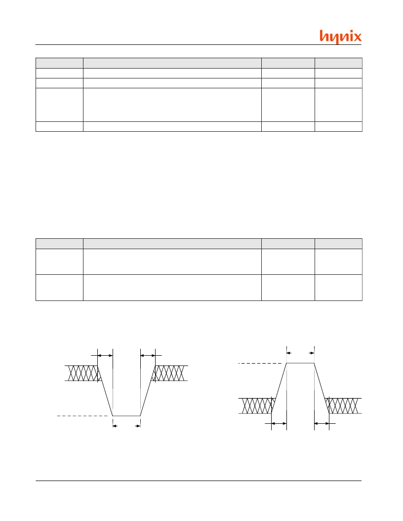
2.0 V
V
CC
+ 0.5 V
V
CC
+ 2.0 V
20 ns
20 ns
20 ns
Figure 9. Maximum Undershoot Waveform
Figure 10. Maximum Overshoot Waveform
0.8 V
- 0.5 V
- 2.0 V
20 ns
20 ns
20 ns
相關(guān)PDF資料 |
PDF描述 |
|---|---|
| HY29LV160BF-80 | 16 Mbit (2M x 8/1M x 16) Low Voltage Flash Memory |
| HY29LV160TF-80 | 16 Mbit (2M x 8/1M x 16) Low Voltage Flash Memory |
| HY29LV160BF-90 | 16 Mbit (2M x 8/1M x 16) Low Voltage Flash Memory |
| HY29LV160TF-90 | 16 Mbit (2M x 8/1M x 16) Low Voltage Flash Memory |
| HY29LV160BF-70I | 16 Mbit (2M x 8/1M x 16) Low Voltage Flash Memory |
相關(guān)代理商/技術(shù)參數(shù) |
參數(shù)描述 |
|---|---|
| HY29LV160TF-70I | 制造商:HYNIX 制造商全稱(chēng):Hynix Semiconductor 功能描述:16 Mbit (2M x 8/1M x 16) Low Voltage Flash Memory |
| HY29LV160TF-80 | 制造商:HYNIX 制造商全稱(chēng):Hynix Semiconductor 功能描述:16 Mbit (2M x 8/1M x 16) Low Voltage Flash Memory |
| HY29LV160TF-80I | 制造商:HYNIX 制造商全稱(chēng):Hynix Semiconductor 功能描述:16 Mbit (2M x 8/1M x 16) Low Voltage Flash Memory |
| HY29LV160TF-90 | 制造商:HYNIX 制造商全稱(chēng):Hynix Semiconductor 功能描述:16 Mbit (2M x 8/1M x 16) Low Voltage Flash Memory |
| HY29LV160TF-90I | 制造商:HYNIX 制造商全稱(chēng):Hynix Semiconductor 功能描述:16 Mbit (2M x 8/1M x 16) Low Voltage Flash Memory |
發(fā)布緊急采購(gòu),3分鐘左右您將得到回復(fù)。