- 您現(xiàn)在的位置:買賣IC網(wǎng) > PDF目錄385425 > HY5DU121622C (Hynix Semiconductor Inc.) 512Mb DDR SDRAM PDF資料下載
參數(shù)資料
| 型號(hào): | HY5DU121622C |
| 廠商: | Hynix Semiconductor Inc. |
| 英文描述: | 512Mb DDR SDRAM |
| 中文描述: | 產(chǎn)品512Mb DDR SDRAM |
| 文件頁(yè)數(shù): | 19/31頁(yè) |
| 文件大?。?/td> | 253K |
| 代理商: | HY5DU121622C |
第1頁(yè)第2頁(yè)第3頁(yè)第4頁(yè)第5頁(yè)第6頁(yè)第7頁(yè)第8頁(yè)第9頁(yè)第10頁(yè)第11頁(yè)第12頁(yè)第13頁(yè)第14頁(yè)第15頁(yè)第16頁(yè)第17頁(yè)第18頁(yè)當(dāng)前第19頁(yè)第20頁(yè)第21頁(yè)第22頁(yè)第23頁(yè)第24頁(yè)第25頁(yè)第26頁(yè)第27頁(yè)第28頁(yè)第29頁(yè)第30頁(yè)第31頁(yè)
Rev. 1.0 / Mar. 2005
19
1
HY5DU12422C(L)TP
HY5DU12822C(L)TP
HY5DU121622C(L)TP
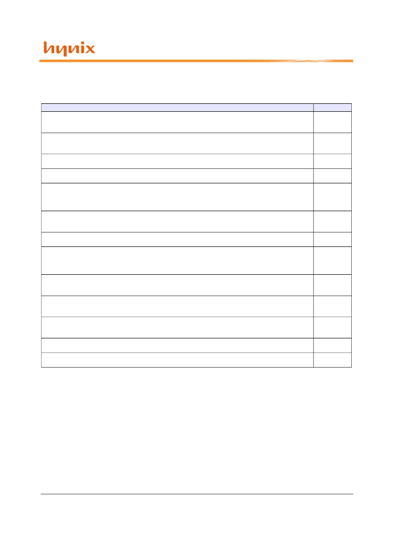
IDD SPECIFICATION AND CONDITIONS
(TA=0 to 70
o
C, Voltage referenced to V
SS
= 0V)
Test Conditions
Test Condition
Symbol
Operating Current:
One bank; Active - Precharge; tRC=tRC(min); tCK=tCK(min); DQ,DM and DQS inputs changing twice per clock
cycle; address and control inputs changing once per clock cycle
Operating Current:
One bank; Active - Read - Precharge;
Burst Length=2; tRC=tRC(min); tCK=tCK(min); address and control inputs changing once per clock cycle
Precharge Power Down Standby Current:
All banks idle; Power down mode; CKE=Low, tCK=tCK(min)
Idle Standby Current:
Vin>=Vih(min) or Vin=<Vil(max) for DQ, DQS and DM
Idle Standby Current:
/CS=High, All banks idle; tCK=tCK(min);
CKE=High; address and control inputs changing once per clock cycle.
VIN=VREF for DQ, DQS and DM
Idle Quiet Standby Current:
/CS>=Vih(min); All banks idle; CKE>=Vih(min); Addresses and other control inputs stable, Vin=Vref for DQ, DQS
and DM
Active Power Down Standby Current:
One bank active; Power down mode; CKE=Low, tCK=tCK(min)
Active Standby Current:
/CS=HIGH; CKE=HIGH; One bank; Active-Precharge; tRC=tRAS(max); tCK=tCK(min);
DQ, DM and DQS inputs changing twice per clock cycle; Address and other control inputs changing once per clock
cycle
Operating Current:
Burst=2; Reads; Continuous burst; One bank active; Address and control inputs changing once per clock cycle;
tCK=tCK(min); IOUT=0mA
Operating Current:
Burst=2; Writes; Continuous burst; One bank active; Address and control inputs changing once per clock cycle;
tCK=tCK(min); DQ, DM and DQS inputs changing twice per clock cycle
Auto Refresh Current:
tRC=tRFC(min) - 8*tCK for DDR200 at 100Mhz, 10*tCK for DDR266A & DDR266B at 133Mhz; distributed refresh
tRC=tRFC(min) - 14*tCK for DDR400 at 200Mhz
Self Refresh Current:
CKE =< 0.2V; External clock on; tCK=tCK(min)
Operating Current - Four Bank Operation:
Four bank interleaving with BL=4, Refer to the following page for detailed test condition
IDD0
IDD1
IDD2P
IDD2N
IDD2F
IDD2Q
IDD3P
IDD3N
IDD4R
IDD4W
IDD5
IDD6
IDD7
相關(guān)PDF資料 |
PDF描述 |
|---|---|
| HY5DU121622CLTP | 512Mb DDR SDRAM |
| HY5DU121622CLTP-X | 512Mb DDR SDRAM |
| HY5DU12422C | CAP .039UF 16V PPS FILM SMD |
| HY5DU12422CLTP | CAP.00047UF 16V PPS FILM 0603 2% |
| HY5DU12422CLTP-X | 512Mb DDR SDRAM |
相關(guān)代理商/技術(shù)參數(shù) |
參數(shù)描述 |
|---|---|
| HY5DU121622CFP | 制造商:HYNIX 制造商全稱:Hynix Semiconductor 功能描述:512Mb DDR SDRAM |
| HY5DU121622CLFP | 制造商:HYNIX 制造商全稱:Hynix Semiconductor 功能描述:512Mb DDR SDRAM |
| HY5DU121622CLTP | 制造商:HYNIX 制造商全稱:Hynix Semiconductor 功能描述:512Mb DDR SDRAM |
| HY5DU121622CLTP-X | 制造商:HYNIX 制造商全稱:Hynix Semiconductor 功能描述:512Mb DDR SDRAM |
| HY5DU121622CTP | 制造商:HYNIX 制造商全稱:Hynix Semiconductor 功能描述:512Mb DDR SDRAM |
發(fā)布緊急采購(gòu),3分鐘左右您將得到回復(fù)。