- 您現在的位置:買賣IC網 > PDF目錄360678 > I74F776N (NXP SEMICONDUCTORS) Pi-bus transceiver PDF資料下載
參數資料
| 型號: | I74F776N |
| 廠商: | NXP SEMICONDUCTORS |
| 元件分類: | 通用總線功能 |
| 英文描述: | Pi-bus transceiver |
| 中文描述: | F/FAST SERIES, 8-BIT REGISTERED TRANSCEIVER, TRUE OUTPUT, PDIP28 |
| 封裝: | 0.600 INCH, PLASTIC, DIP-28 |
| 文件頁數: | 7/12頁 |
| 文件大?。?/td> | 108K |
| 代理商: | I74F776N |
Philips Semiconductors
Product specification
74F776
Pi–bus transceiver
December 19, 1990
7
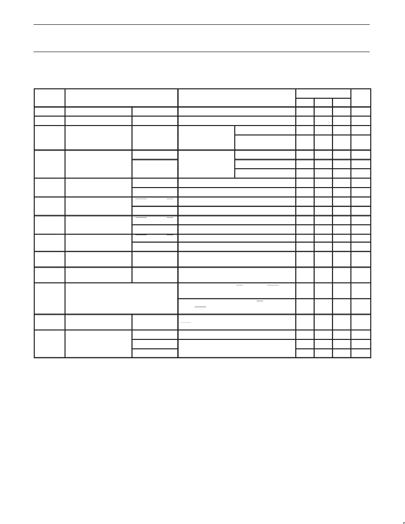
DC ELECTRICAL CHARACTERISTICS
(Over recommended operating free-air temperature range unless otherwise noted.)
SYMBOL
PARAMETER
TEST
LIMITS
TYP
2
UNIT
CONDITIONS
1
MIN
MAX
I
OH
I
OFF
High–level output current
B0 – B7
V
CC
= MAX, V
IL
= MAX, V
IH
= MIN, V
OH
= 2.1V
V
CC
= 0.0V, V
IL
= MAX, V
IH
= MIN, V
OH
= 2.1V
V
CC
= MIN,
100
μ
A
μ
A
Power–off output current
B0 – B7
100
I
OH
= –3mA, V
X
=V
CC
I
OH
= –4mA,
V
X
=3.13V and 3.47V
I
OL
= 20mA, V
X
= V
CC
I
OL
= 100mA
I
OL
= 4mA
2.5
V
CC
V
V
OH
High-level output voltage
A0 – A7
4
V
IL
= MAX, V
IH
= MIN
2.5
V
A0 – A7
4
V
CC
= MIN,
V
IL
= MAX
V
IH
= MIN
V
CC
= MIN, I
I
= I
IK
V
CC
= MIN, I
I
= I
IK
V
CC
= 0.0V, V
I
= 7.0V
V
CC
= MAX, V
I
= 5.5V
V
CC
= MAX, V
I
= 2.7V, Bn –An =0V
V
CC
= MAX, V
I
= 2.1V
V
CC
= MAX, V
I
= 0.5V
V
CC
= MAX, V
I
= 0.3V
0.50
V
V
OL
Low-level output voltage
B0 – B7
1.15
V
0.40
V
V
IK
Input clamp voltage
A0 – A7
-0.5
V
Except A0 – A7
-1.2
V
μ
A
I
I
Input current at
OEBn, OEA, LE
100
maximum input voltage
A0 – A7, B0 – B7
1
mA
I
IH
High–level input current
OEBn, OEA, LE
20
μ
A
μ
A
μ
A
μ
A
B0 – B7
100
–20
I
IL
Low–level input current
OEBn, OEA, LE
B0 – B7
–100
I
OZH
+ I
IH
Off state output current,
high level voltage applied
A0 – A7
V
CC
= MAX, V
O
= 2.7V
70
μ
A
I
OZL
+ I
IL
Off state output current,
low level voltage applied
A0 – A7
V
CC
= MAX, V
O
= 0.5V
–70
μ
A
I
X
High–level control current
V
CC
= MAX, V
X
= V
CC
, LE = OEA
= OEBn
=
2.7V, A0 – A7 = 2.7V, B0 – B7 = 2.0V,
–100
100
μ
A
V
CC
= MAX, V
X
= 3.13 & 3.47V, LE = OEA
=
2.7V, OEBn
= A0 – A7 = 2.7V, B0 – B7 = 2.0V,
–10
10
μ
A
I
OS
Short circuit output
current
3
A0 – A7
only
V
= MAX, Bn = 1.8V, OEA = 2.0V,
OEBn
= 2.7V
-60
-150
mA
I
CCH
I
CCL
I
CCZ
V
CC
= MAX
V
CC
= MAX, V
IL
= 0.5V
65
100
mA
I
CC
Supply current (total)
100
145
mA
75
100
mA
Notes to DC electrical characteristics
1. For conditions shown as MIN or MAX, use the appropriate value specified under recommended operating conditions for the applicable type.
Unless otherwise specified, V
X
= V
CC
for all test conditions.
2. All typical values are at V
CC
= 5V, T
amb
= 25
°
C.
3. Not more than one output should be shorted at a time. For testing I
OS
, the use of high-speed test apparatus and/or sample-and-hold
techniques are preferable in order to minimize internal heating and more accurately reflect operational values. Otherwise, prolonged shorting
of a high output may raise the chip temperature well above normal and thereby cause invalid readings in other parameter tests. In any
sequence of parameter tests, I
OS
tests should be performed last.
4. Due to test equipment limitations, actual test conditions are for V
IH
=1.8v and V
IL
= 1.3V.
相關PDF資料 |
PDF描述 |
|---|---|
| I74F777A | Triple bidirectional latched bus transceiver 3-State open collector |
| I74F777N | Triple bidirectional latched bus transceiver 3-State open collector |
| I74F86D-T | Quad 2-input Exclusive OR (XOR) Gate |
| 74F86DC | Quad 2-input Exclusive OR (XOR) Gate |
| 74F86SCX | Quad 2-input Exclusive OR (XOR) Gate |
相關代理商/技術參數 |
參數描述 |
|---|---|
| I74F776N-B | 制造商:未知廠家 制造商全稱:未知廠家 功能描述:8-Bit Inverting/Non-Inverting Bus Trasceiver |
| I74F777A | 制造商:PHILIPS 制造商全稱:NXP Semiconductors 功能描述:Triple bidirectional latched bus transceiver 3-State open collector |
| I74F777AB | 制造商:未知廠家 制造商全稱:未知廠家 功能描述:1-Bit Bus Transceiver |
| I74F777N | 制造商:PHILIPS 制造商全稱:NXP Semiconductors 功能描述:Triple bidirectional latched bus transceiver 3-State open collector |
| I74F777N-B | 制造商:未知廠家 制造商全稱:未知廠家 功能描述:1-Bit Bus Transceiver |
發(fā)布緊急采購,3分鐘左右您將得到回復。