- 您現(xiàn)在的位置:買賣IC網(wǎng) > PDF目錄67682 > IBM25NPE405L-3FA200CZ 32-BIT, 200 MHz, RISC PROCESSOR, PBGA324 PDF資料下載
參數(shù)資料
| 型號: | IBM25NPE405L-3FA200CZ |
| 元件分類: | 微控制器/微處理器 |
| 英文描述: | 32-BIT, 200 MHz, RISC PROCESSOR, PBGA324 |
| 封裝: | 23 X 23 MM, PLASTIC, EBGA-324 |
| 文件頁數(shù): | 42/52頁 |
| 文件大小: | 907K |
| 代理商: | IBM25NPE405L-3FA200CZ |
第1頁第2頁第3頁第4頁第5頁第6頁第7頁第8頁第9頁第10頁第11頁第12頁第13頁第14頁第15頁第16頁第17頁第18頁第19頁第20頁第21頁第22頁第23頁第24頁第25頁第26頁第27頁第28頁第29頁第30頁第31頁第32頁第33頁第34頁第35頁第36頁第37頁第38頁第39頁第40頁第41頁當(dāng)前第42頁第43頁第44頁第45頁第46頁第47頁第48頁第49頁第50頁第51頁第52頁
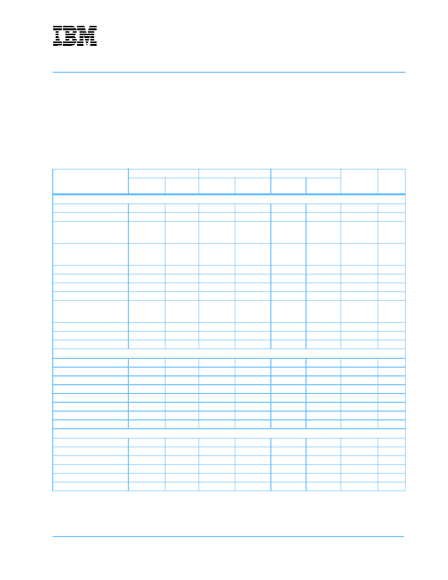
Preliminary
PowerNP NPe405L Embedded Processor Data Sheet
47
I/O Specifications—133 and 200MHz (Part 1 of 2)
Notes:
1. Ethernet interface meets timing requirements as defined by IEEE 802.3 standard.
2. The SDRAM command interface is configurable through SDRAM0_TR[LDF] to provide a 2 to 4 cycle delay before the
command is used by SDRAM. Output times in table are in cycle 1.
3. SDRAM I/O timings are specified relative to a SysClk terminated in a lumped 10pF load.
4. SDRAM interface hold times are guaranteed at the NPe405L package pin. System designers must use the NPe405L
IBIS model (available from www.chips.ibm.com) to ensure their clock distribution topology minimizes loading and
reflections, and that the relative delays on clock wiring do not exceed the delays on other SDRAM signal wiring.
5. PerClk rising edge at package pin with a 10pF load trails the internal PLB clock by approximately 0.8ns.
Signal
Input (ns)
Output (ns)
Output Current (mA)
Clock
Notes
Setup Time
(TIS min)
Hold Time
TIH min)
Valid Delay
(TOV max)
Hold Time
(TOH min)
I/O H
(maximum)
I/O L
(minimum)
Ethernet Interface
EMC0MDClk
n/a
7.4
1.5
12
8
1, async
EMC0MDIO
n/a
8.8
1.2
12
8
EMC0MDClk
1
EMC0TxD0:3
[EMC0Tx0:1D0:1]
[EMC0Tx0:1D]
n/a
10.5
[7.3]
[5.0]
3.0
[2.3]
[1.7]
12
8
PHYTX
1
EMC0TxEn
[EMC0Tx0En]
[EMC0Sync]
n/a
11.8
[7.2]
[5.6]
2.9
[2.3]
[1.7]
12
8
PHYTX
1
EMC0TxErr[EMC0Tx1En]
n/a
11.8[7.4]
2.9[2.4]
12
8
PHYTX
1
PHY0Col[PHY0Rx1Er]
async[0.2]
async[1.7]
n/a
1
PHY0CrS[PHY0CrS0DV]
async[0.1]
async[1.9]
n/a
1
PHY0RxClk
n/a
1, async
PHY0RxD0:3
[PHY0Rx0:1D0:1]
[PHY0Rx0:1D]
1.5
[0.8]
[0.9]
1.7
[1.7]
[0.3]
n/a
PHYRX
1
PHY0RxDV[PHY0CRS1DV]
1.3[0.7]
1.7[1.7]
n/a
PHYRX
1
PHY0RxErr[PHY0Rx0Er]
1.3[0.7]
1.8[1.9]
n/a
PHYRX
1
PHY0TxClk[PHY0RefClk]
n/a
1, async
HDLCEX Interface
HDLCEXRxClk
n/a
HDLCEXRxDataA:B
23.8
2.1
n/a
HDLCEXRxFS
24.2
1.1
n/a
HDLCEXTxClk
n/a
HDLCEXTxDataA:B
n/a
10.5
3.3
12
8
HDLCEXTxFS
20.3
1.0
n/a
[HDLCEXTxEnA]
n/a
11.3
3.5
12
8
[HDLCEXTxEnB]]
n/a
11.8
3.8
12
8
Trace Interface
[TrcClk]GPIO00
n/a
11.2
1.2
12
8
[TS1E]GPIO01
n/a
7.0
1.2
12
8
[TS2E]GPIO02
n/a
7.0
1.2
12
8
[TS1O]GPIO03
n/a
6.5
1.0
12
8
[TS2O]GPIO04
n/a
6.4
1.0
12
8
[TS3:6]GPIO05:08
n/a
6.4
1.0
12
8
相關(guān)PDF資料 |
PDF描述 |
|---|---|
| IBM25NPE405L-3FA266CZ | 32-BIT, 266 MHz, RISC PROCESSOR, PBGA324 |
| IBM25PPC405EP-3GB133CZ | 32-BIT, 133.33 MHz, RISC PROCESSOR, PBGA385 |
| IBM25PPC405EP-3GB133C | 32-BIT, 133.33 MHz, RISC PROCESSOR, PBGA385 |
| IBM25PPC405GP-3DD200C | RISC PROCESSOR, PBGA456 |
| IBM25PPC405GP-3BD266C | RISC PROCESSOR, PBGA456 |
相關(guān)代理商/技術(shù)參數(shù) |
參數(shù)描述 |
|---|---|
| IBM25NPE405L-3FA266C | 制造商:AMCC 制造商全稱:Applied Micro Circuits Corporation 功能描述:PowerNP |
| IBM25NPE405L-3FA266CZ | 制造商:AMCC 制造商全稱:Applied Micro Circuits Corporation 功能描述:PowerNP |
| IBM25PPC403GAJC33C1 | 制造商:IBM 功能描述: |
| IBM25PPC405CR-3BC200C | 制造商:未知廠家 制造商全稱:未知廠家 功能描述:MICROPROCESSOR|32-BIT|CMOS|BGA|316PIN|PLASTIC |
| IBM25PPC405CR-3BC200CZ | 制造商:未知廠家 制造商全稱:未知廠家 功能描述:MICROPROCESSOR|32-BIT|CMOS|BGA|316PIN|PLASTIC |
發(fā)布緊急采購,3分鐘左右您將得到回復(fù)。