- 您現(xiàn)在的位置:買賣IC網(wǎng) > PDF目錄383086 > ICL7641ECPD (HARRIS SEMICONDUCTOR) Dual/Quad, Low Power CMOS Operational Amplifiers PDF資料下載
參數(shù)資料
| 型號(hào): | ICL7641ECPD |
| 廠商: | HARRIS SEMICONDUCTOR |
| 元件分類: | 運(yùn)動(dòng)控制電子 |
| 英文描述: | Dual/Quad, Low Power CMOS Operational Amplifiers |
| 中文描述: | QUAD OP-AMP, 25000 uV OFFSET-MAX, 1.4 MHz BAND WIDTH, PDIP14 |
| 文件頁(yè)數(shù): | 2/9頁(yè) |
| 文件大?。?/td> | 80K |
| 代理商: | ICL7641ECPD |
2
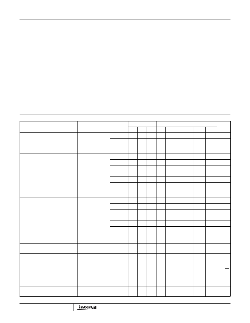
Absolute Maximum Ratings
Thermal Information
Supply Voltage V+ to V-. . . . . . . . . . . . . . . . . . . . . . . . . . . . . . . .18V
Input Voltage . . . . . . . . . . . . . . . . . . . . . . . . . . . V- -0.3 to V+ +0.3V
Differential Input Voltage (Note 1) . . . . . . . . . [(V+ +0.3) - (V- -0.3)]V
Duration of Output Short Circuit (Note 2). . . . . . . . . . . . . . Unlimited
Operating Conditions
Temperature Range
ICL76XXM . . . . . . . . . . . . . . . . . . . . . . . . . . . . . . -55
o
C to 125
o
C
ICL76XXC . . . . . . . . . . . . . . . . . . . . . . . . . . . . . . . . 0
o
C to 70
o
C
Thermal Resistance (Typical, Note 3)
SOIC Package . . . . . . . . . . . . . . . . . . .
Metal Can Package . . . . . . . . . . . . . . .
8 Lead PDIP Package . . . . . . . . . . . . .
14 Lead PDIP Package . . . . . . . . . . . .
Maximum Junction Temperature (Hermetic Packages). . . . . . . .175
o
C
Maximum Junction Temperature (Plastic Package) . . . . . . . .150
o
C
Maximum Storage Temperature Range. . . . . . . . . . -65
o
C to 150
o
C
Maximum Lead Temperature (Soldering 10s) . . . . . . . . . . . . 300
o
C
(SOIC - Lead Tips Only)
θ
JA
(
o
C/W)
160
160
120
80
θ
JC
(
o
C/W)
N/A
75
N/A
N/A
CAUTION: Stresses above those listed in “Absolute Maximum Ratings” may cause permanent damage to the device. This is a stress only rating and operation of the
device at these or any other conditions above those indicated in the operational sections of this specification is not implied.
NOTES:
1. Long term offset voltage stability will be degraded if large input differential voltages are applied for long periods of time.
2. The outputs may be shorted to ground or to either supply, for V
SUPPLY
≤
10V. Care must be taken to insure that the dissipation rating is not
exceeded.
3.
θ
JA
is measured with the component mounted on an evaluation PC board in free air.
Electrical Specifications
V
SUPPLY
=
±
5V, Unless Otherwise Specified
PARAMETER
SYMBOL
TEST
CONDITIONS
TEMP.
(
o
C)
ICL7621A
ICL7621B
ICL7621D
UNITS
MIN
TYP MAX MIN
TYP MAX MIN
TYP
MAX
Input Offset Voltage
V
OS
R
S
≤
100k
25
-
-
2
-
-
5
-
-
15
mV
Full
-
-
-
3
-
-
7
-
-
20
mV
μ
V/
o
C
Temperature
Coefficient of V
OS
Input Offset Current
V
OS
/
T R
S
≤
100k
-
10
-
-
15
-
-
25
-
I
OS
25
-
0.5
30
-
0.5
30
-
0.5
30
pA
0 to 70
-
-
300
-
-
300
-
-
300
pA
-55 to 125
-
-
800
-
800
-
800
pA
Input Bias Current
I
BIAS
25
-
1.0
50
-
1.0
50
-
1.0
50
pA
0 to 70
-
-
400
-
-
400
-
-
400
pA
-55 to 125
-
-
4000
-
-
4000
-
-
4000
pA
Common Mode Voltage
Range
V
CMR
I
Q
= 100
μ
A
25
±
4.2
-
-
±
4.2
-
-
±
4.2
-
-
V
Output Voltage Swing
V
OUT
I
Q
= 100
μ
A,
R
L
= 100k
25
±
4.9
±
4.8
±
4.5
-
-
±
4.9
±
4.8
±
4.5
-
-
±
4.9
±
4.8
±
4.5
-
-
V
0 to 70
-
-
-
-
-
-
V
-55 to 125
-
-
-
-
-
-
V
Large Signal
Voltage Gain
A
VOL
V
O
=
±
4.0V,
R
L
= 100k
,
I
Q
= 100
μ
A
25
86
102
-
80
102
-
80
102
-
dB
0 to 70
80
-
-
75
-
-
75
-
-
dB
-55 to 125
74
-
-
68
-
-
68
-
-
dB
Unity Gain Bandwidth
GBW
I
Q
= 100
μ
A
25
-
0.48
10
12
-
-
0.48
10
12
-
-
0.48
10
12
-
MHz
Input Resistance
R
IN
CMRR
25
-
-
-
-
-
-
Common Mode
Rejection Ratio
R
S
≤
100k
,
I
Q
= 100
μ
A
R
S
≤
100k
,
I
Q
= 100
μ
A
25
76
91
-
70
91
-
70
91
-
dB
Power Supply
Rejection Ratio
(V
SUPPLY
=
±
8V to
±
2V)
Input Referred Noise
Voltage
PSRR
25
80
86
-
80
86
-
80
86
-
dB
e
N
R
S
= 100
,
f = 1kHz
25
-
100
-
-
100
-
-
100
-
nV/
√
Hz
Input Referred Noise
Current
i
N
R
S
= 100
,
f = 1kHz
25
-
0.01
-
-
0.01
-
-
0.01
-
pA/
√
Hz
Supply Current
(Per Amplifier)
I
SUPPLY
No Signal, No Load,
I
Q
= 100
μ
A
25
-
0.1
0.25
-
0.1
0.25
-
0.1
0.25
mA
ICL7621, ICL7641, ICL7642
相關(guān)PDF資料 |
PDF描述 |
|---|---|
| ICL7642 | High-Performance Impact-X<TM> PAL<R> Circuits 20-CFP -55 to 125 |
| ICL7642ECPD | High-Performance Impact-X<TM> PAL<R> Circuits 20-CFP -55 to 125 |
| ICL7641 | Dual, Low Power CMOS Operational Amplifiers(雙路低功耗CMOS放大器) |
| ICL7650B | Chopper-Stabilized Op Amps |
| ICL7653 | Chopper-Stabilized Op Amps |
相關(guān)代理商/技術(shù)參數(shù) |
參數(shù)描述 |
|---|---|
| ICL7641ECPD WAF | 制造商:Harris Corporation 功能描述: 制造商:Intersil Corporation 功能描述: |
| ICL7641ECPD+ | 功能描述:運(yùn)算放大器 - 運(yùn)放 Quad CMOS Low Power RoHS:否 制造商:STMicroelectronics 通道數(shù)量:4 共模抑制比(最小值):63 dB 輸入補(bǔ)償電壓:1 mV 輸入偏流(最大值):10 pA 工作電源電壓:2.7 V to 5.5 V 安裝風(fēng)格:SMD/SMT 封裝 / 箱體:QFN-16 轉(zhuǎn)換速度:0.89 V/us 關(guān)閉:No 輸出電流:55 mA 最大工作溫度:+ 125 C 封裝:Reel |
| ICL7641ECPD-2 | 制造商:Maxim Integrated Products 功能描述: |
| ICL7641ECWE | 功能描述:運(yùn)算放大器 - 運(yùn)放 RoHS:否 制造商:STMicroelectronics 通道數(shù)量:4 共模抑制比(最小值):63 dB 輸入補(bǔ)償電壓:1 mV 輸入偏流(最大值):10 pA 工作電源電壓:2.7 V to 5.5 V 安裝風(fēng)格:SMD/SMT 封裝 / 箱體:QFN-16 轉(zhuǎn)換速度:0.89 V/us 關(guān)閉:No 輸出電流:55 mA 最大工作溫度:+ 125 C 封裝:Reel |
| ICL7641ECWE+ | 功能描述:運(yùn)算放大器 - 運(yùn)放 Quad CMOS Low Power RoHS:否 制造商:STMicroelectronics 通道數(shù)量:4 共模抑制比(最小值):63 dB 輸入補(bǔ)償電壓:1 mV 輸入偏流(最大值):10 pA 工作電源電壓:2.7 V to 5.5 V 安裝風(fēng)格:SMD/SMT 封裝 / 箱體:QFN-16 轉(zhuǎn)換速度:0.89 V/us 關(guān)閉:No 輸出電流:55 mA 最大工作溫度:+ 125 C 封裝:Reel |
發(fā)布緊急采購(gòu),3分鐘左右您將得到回復(fù)。