- 您現(xiàn)在的位置:買賣IC網(wǎng) > PDF目錄360744 > ICS1886M FDDI / Fast Ethernet PHYceiverTM PDF資料下載
參數(shù)資料
| 型號(hào): | ICS1886M |
| 英文描述: | FDDI / Fast Ethernet PHYceiverTM |
| 中文描述: | FDDI的/快速以太網(wǎng)PHYceiverTM |
| 文件頁(yè)數(shù): | 6/10頁(yè) |
| 文件大小: | 726K |
| 代理商: | ICS1886M |
6
ICS1886
Input Pin Descriptions
Transmit Data Input (TD+ and TD-) For normal operation
this differential input is transferred to the TX
±
output
through a PECL buffer. In loopback testing mode, this input
is multiplexed to the input of the device clock recovery
section.
Receive Data Input (RX+ and RX-)
The clock recovery
and data regenerator from the receive buffer are driven from
this PECL input. During loopback testing mode this input is
ignored.
Clock Select (CS0 and CS1)
Selects the operating
frequency according to Table 1. Internal pull-up resistors
set both inputs high when left unconnected.
Carrier Detect (CD~)
Active low input which forces the
VCO to free run. Upon receipt of a loss of input signal
(such as from an optical-to-elec-trical transducer), the
internal phase-lock loop will free-run at the selected
operating frequency. Also, when asserted, CD will set the
lock output low.
Loop Timing Mode (LT~)
Active low input which routes
the recovered receive clock to the TC
±
outputs as well as
the RC
±
outputs. Forces the transmit clock to be loop-
timed to the system clock derived from the incoming data.
Loopback Mode (LB~)
Active low input which causes the
clock recovery PLL to operate using the transmit TD
±
input
data and ignore the receive RX
±
data. Utilized for system
loopback testing.
External Crystal or Reference Clock (REF+ and REF-)
This oscillator input can be driven from either a
fundamental mode crystal or a stable reference. For either
method, the reference frequency is
1
8
the operating
frequency. See Table 1 for more information.
Output Pin Descriptions
Transmit Data Differential
ECL (TX+ and TX-) This differential output is buffered TD
±
data. This output remains active during loopback mode.
Transmit Clock Differential ECL (TC+ and TC-)
Differential output clock used by the PDH/ATM processor
for clocking out transmit data. This clock can be derived
from either an independent clock source
or
from the
recovered data clock (system loop time mode).
Receive Data Differential ECL (RD+ and RD-)
The
regenerated differential data derived from the serial data
input. In loopback mode this data is regenerated from the
transmit data input (TD
±
). This data is phase-aligned with
the negative edge of the RC clock output.
Receive Clock Differential ECL (RC+ and RC-)
The
differential clock recovered with the internal clock recov-
ery PLL. In loopback mode this clock is recovered from the
transmit data (TD
±
) input. This clock is phase-aligned with
the RD data output.
Lock/Loss Detect (LOCK)
Set high when the clock
recovery PLL has locked onto the incoming data. Set low
when there is no incoming data, which in turn causes the
PLL to free-run. This signal can be used to indicate or
alarm the next receive stage that the incoming serial data
has stopped.
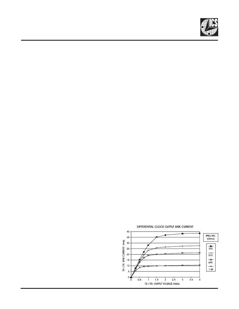
Output Description
The differential output drivers are current mode and are de-
signed to drive resistive terminations in a complementary
fash-ion. The outputs are current-sinking only, with the
amount of sink current programmable via the
IPRGx
pins.
The sink current is equal to four times the IPRGx current.
For most applications, a resistor from VDD to IPRGx will
set the current to the necessary precision.
IPRG1
supplies
the current mirror for the TX
±
output.
IPRG2
supplies the
current mirrors for the RD
±
, RC
±
and TC
±
outputs.
The differential PECL output pins are incapble of sourcing
current, so V
OH
must be set by the ratios of the termination
resistors for each of these lines. R1 is a pull-up resistor
con-nected from the PECL output to VSS. R1 and R2 are
electrically in parallel from an AC stand point. If we pick a
target imped-ance of 50
for our transmission line
impedance, a value of 62
for R1 and a value of 300
for
R2 would yield a Thevenin equivalent characteristic
impedance of 50
and a V
OH
value of V
DD
-.88 volts,
compatible with PECL circuits.
To set a value for V
OL
, we must determine a value for Iprg
that will cause the output FETs to sink an appropriate
current. We desire V
OL
to be V
DD
-1.81 or greater. Setting
up a sink current of 19 milliamperes would guarantee this
through out output terminating resistors. As this is
controlled by a 4/1 current mirror, 4.75mA into Iprg should
set this current properly. An 910
resistor from V
DD
to
Iprg should work fine.
相關(guān)PDF資料 |
PDF描述 |
|---|---|
| ICS1887 | FDDI / Fast Ethernet PHYceiverTM |
| ICS1887M | FDDI / Fast Ethernet PHYceiverTM |
| ICS1889 | 100Base-FX Integrated PHYceiverTM |
| ICS1892 | 10Base-T/100Base-TX Integrated PHYceiver |
| ICS1892Y | 10Base-T/100Base-TX Integrated PHYceiver |
相關(guān)代理商/技術(shù)參數(shù) |
參數(shù)描述 |
|---|---|
| ICS1887 | 制造商:ICS 制造商全稱:ICS 功能描述:FDDI / Fast Ethernet PHYceiverTM |
| ICS1887M | 制造商:ICS 制造商全稱:ICS 功能描述:FDDI / Fast Ethernet PHYceiverTM |
| ICS1888 | 制造商:未知廠家 制造商全稱:未知廠家 功能描述:ATM/SONET Transceiver |
| ICS1889 | 制造商:ICS 制造商全稱:ICS 功能描述:100Base-FX Integrated PHYceiverTM |
| ICS1890 | 制造商:ICS 制造商全稱:ICS 功能描述:Auto-Negotiation Advertisement Register (register 4 [0x04]) |
發(fā)布緊急采購(gòu),3分鐘左右您將得到回復(fù)。