- 您現在的位置:買賣IC網 > PDF目錄360752 > ICS650-22 PVR and STB Clock Source PDF資料下載
參數資料
| 型號: | ICS650-22 |
| 英文描述: | PVR and STB Clock Source |
| 中文描述: | PVR和機頂盒時鐘源 |
| 文件頁數: | 3/5頁 |
| 文件大小: | 97K |
| 代理商: | ICS650-22 |
PVR and STB Clock Source
MDS 650-22 D
3
Revision 051004
Integrated Circuit Systems, Inc.
●
525 Race Street, San Jose, CA 95126
●
tel (408) 297-1201
●
www.icst.com
ICS650-22
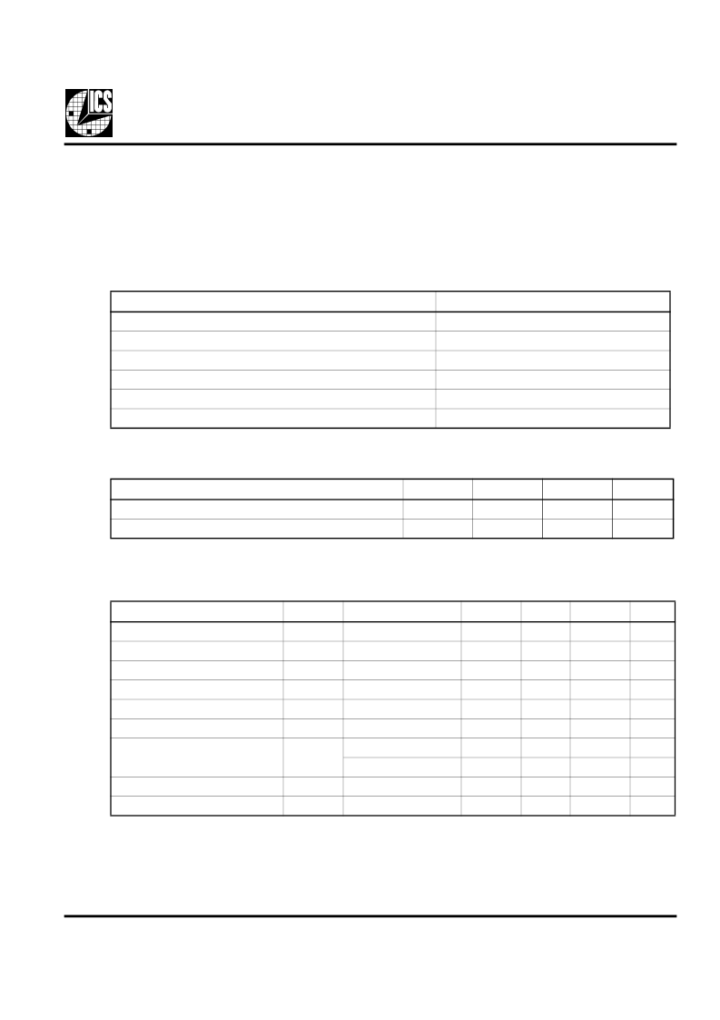
Absolute Maximum Ratings
Stresses above the ratings listed below can cause permanent damage to the ICS650-22. These ratings,
which are standard values for ICS commercially rated parts, are stress ratings only. Functional operation of
the device at these or any other conditions above those indicated in the operational sections of the
specifications is not implied. Exposure to absolute maximum rating conditions for extended periods can
affect product reliability. Electrical parameters are guaranteed only over the recommended operating
temperature range.
Recommended Operation Conditions
DC Electrical Characteristics
Unless stated otherwise,
VDD = 3.3V ±10%
, Ambient Temperature 0 to +70
°
C
Parameter
Symbol
Operating Voltage
VDD
Input High Voltage
V
IH
Input Low Voltage
V
IL
Output High Voltage
V
OH
Output Low Voltage
V
OL
Output High Voltage
V
OL
Operating Supply Current
I
DD
Item
Rating
Supply Voltage, VDD
All Inputs and Outputs
Ambient Operating Temperature
Storage Temperature
Junction Temperature
Soldering Temperature
7 V
-0.5 V to VDD+0.5 V
-40 to +85
°
C
-65 to +150
°
C
125
°
C
260
°
C
Parameter
Ambient Operating Temperature
Power Supply Voltage (measured in respect to GND)
Min.
0
+3.0
Typ.
-
+3.3
Max.
+70
+3.6
Units
°
C
V
Conditions
Min.
3.0
VDD/2+1
Typ.
3.3
VDD/2
VDD/2
Max.
3.6
Units
V
V
V
V
V
V
mA
mA
mA
k
VDD/2-1
I
OH
= -25 mA
I
OL
= +25 mA
I
OH
= -8 mA
No Load, OE=1
No Load, OE=0
Each output
Input select
2.4
0.5
VDD-0.4
29
13
±70
390
Short Circuit Current
Internal Pull-up Resistor
I
OS
R
PU
相關PDF資料 |
PDF描述 |
|---|---|
| ICS650R-22 | PVR and STB Clock Source |
| ICS650R-22LF | PVR and STB Clock Source |
| ICS650R-22LFT | PVR and STB Clock Source |
| ICS650R-22T | PVR and STB Clock Source |
| ICS650-27 | Networking Clock Source |
相關代理商/技術參數 |
參數描述 |
|---|---|
| ICS650-27 | 制造商:ICS 制造商全稱:ICS 功能描述:Networking Clock Source |
| ICS650-36 | 制造商:ICS 制造商全稱:ICS 功能描述:Networking & PCI Clock Source |
| ICS650-40 | 制造商:ICS 制造商全稱:ICS 功能描述:ETHERNET SWITCH CLOCK SOURCE |
| ICS650-40A | 制造商:ICS 制造商全稱:ICS 功能描述:ETHERNET SWITCH CLOCK SOURCE |
| ICS650-41 | 制造商:ICS 制造商全稱:ICS 功能描述:Spread Spectrum Clock Synthesizer |
發(fā)布緊急采購,3分鐘左右您將得到回復。