- 您現(xiàn)在的位置:買賣IC網(wǎng) > PDF目錄360761 > ICS83840AH DDR SDRAM MUX PDF資料下載
參數(shù)資料
| 型號(hào): | ICS83840AH |
| 英文描述: | DDR SDRAM MUX |
| 中文描述: | DDR SDRAM的復(fù)用 |
| 文件頁數(shù): | 1/8頁 |
| 文件大?。?/td> | 139K |
| 代理商: | ICS83840AH |
83840AH
www.icst.com/products/hiperclocks.html
REV. A DECEMBER 22, 2003
1
Integrated
Circuit
Systems, Inc.
ICS83840
DDR SDRAM MUX
G
ENERAL
D
ESCRIPTION
The ICS83840 is a DDR SDRAM MUX and is
a member of the HiPerClockS family of High
Performance Clock Solutions from ICS. The
device has 10 Host Lines and each host line can
be passed to 4 Data Ports. The 10 channels are
allocated as follows in the DDR SDRAM application: 8 data
lines, 1 strobe line and 1 DQm line. The Host/Data Ports are
compatible with single-ended SSTL-2 and the device oper-
ates from a 2.5V supply.
Guaranteed low output skew makes the ICS83840 ideal for
demanding applications which require well defined perfor-
mance and repeatability.
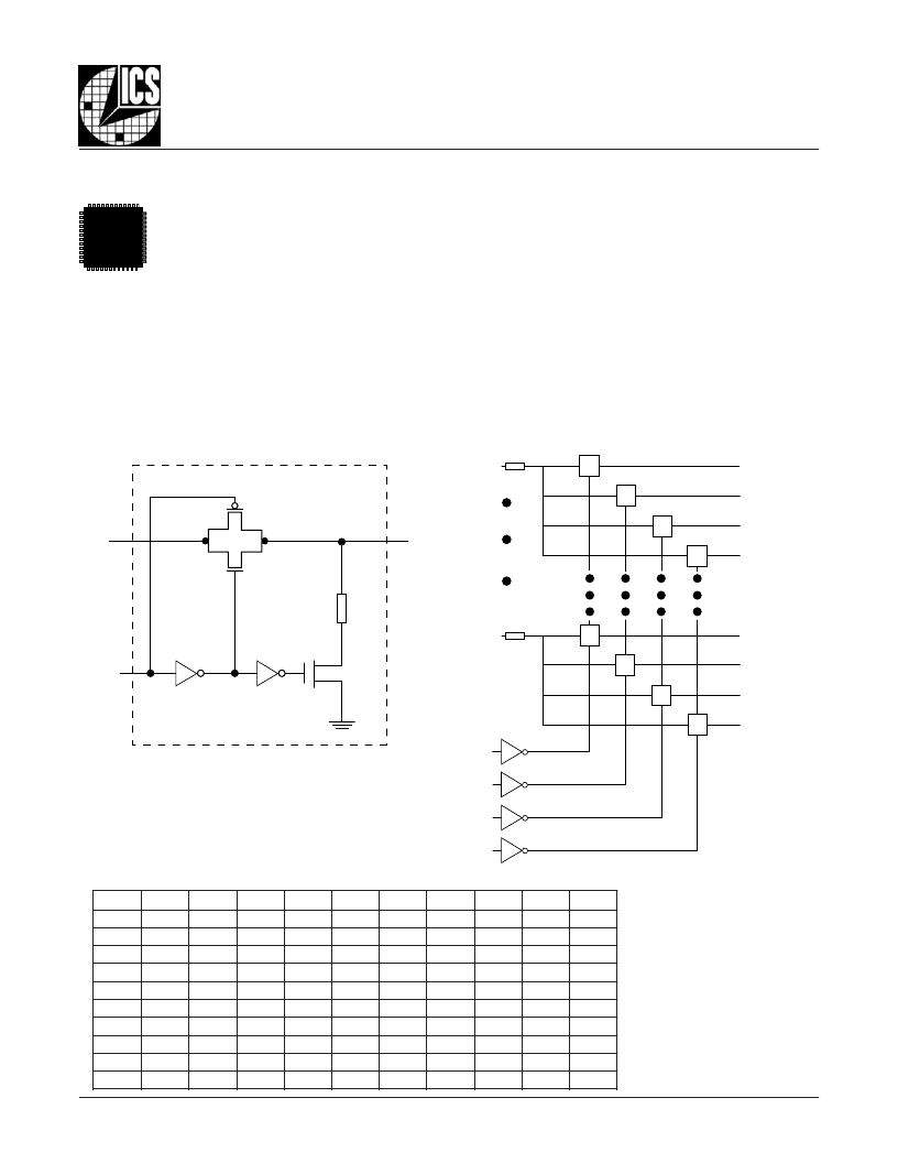
S
IMPLIFIED
S
CHEMATIC
L
OGIC
D
IAGRAM
R
ON
F
EATURES
40 low skew single-ended DIMM ports
4 SSTL-2 compatible enable inputs
Maximum Switching Speed: 3ns
Output skew: 120ps (maximum)
Bank skew: 45ps (maximum)
r
on
= 8
(typical)
Full 2.5V supply modes
0°C to 70°C ambient operating temperature
Pin compatible with the CBTV4010
HiPerClockS
ICS
HPx
nSn
nDPx
SW
400
HP0
0DP0
1DP0
2DP0
3DP0
HP9
Sw
Sw
Sw
Sw
0DP9
1DP9
2DP9
3DP9
Sw
Sw
Sw
Sw
nS0
nS1
nS2
nS3
R
ON
ICS83840
64-Ball TFBGA
7mm x 7mm x 1.2mm
package body
H Package
Top View
P
IN
A
SSIGNMENT
V
n
n
D
2
c
D
1
S
n
V
n
G
D
3
H
D
3
D
2
H
G
D
2
c
n
S
n
0
0
P
P
D
D
1
0
0
0
P
P
D
H
2
0
1
P
P
D
D
3
0
1
1
P
P
D
H
2
1
P
D
N
P
H
P
D
3
D
0
P
H
N
G
D
0
P
H
D
3
D
1
D
3
G
2
2
2
P
P
P
D
D
D
0
1
2
S
D
3
D
9
P
9
P
P
P
8
P
D
N
P
D
0
D
N
G
1
P
D
1
S
N
2
2
3
3
D
4
P
4
P
P
9
9
9
P
P
P
D
D
D
2
1
0
P
3
3
3
P
P
P
D
D
D
1
2
3
8
8
8
8
7
P
P
P
D
D
D
1
0
3
4
4
5
P
P
P
D
D
D
1
2
0
7
P
P
D
H
1
7
P
D
0
6
6
P
P
D
D
3
2
6
P
P
D
H
1
D
6
P
N
G
0
5
P
D
3
5
5
P
P
H
D
2
4
5
7
7
6
D
1
2
3
4
5
6
7
8
9
10
11
A
B
C
D
E
F
G
H
J
K
L
相關(guān)PDF資料 |
PDF描述 |
|---|---|
| ICS83840AHT | DDR SDRAM MUX |
| ICS83840 | Replaced by SN65MLVD205A : Full-Duplex M-LVDS Transceiver 14-SOIC -40 to 85 |
| ICS83840AHLF | DDR SDRAM MUX |
| ICS83840AHLFT | DDR SDRAM MUX |
| ICS83840B | DDR SDRAM MUX |
相關(guān)代理商/技術(shù)參數(shù) |
參數(shù)描述 |
|---|---|
| ICS83840AHLF | 制造商:ICS 制造商全稱:ICS 功能描述:DDR SDRAM MUX |
| ICS83840AHLFT | 制造商:ICS 制造商全稱:ICS 功能描述:DDR SDRAM MUX |
| ICS83840AHT | 制造商:ICS 制造商全稱:ICS 功能描述:DDR SDRAM MUX |
| ICS83840B | 制造商:ICS 制造商全稱:ICS 功能描述:DDR SDRAM MUX |
| ICS83840BH | 制造商:ICS 制造商全稱:ICS 功能描述:DDR SDRAM MUX |
發(fā)布緊急采購,3分鐘左右您將得到回復(fù)。