- 您現(xiàn)在的位置:買賣IC網(wǎng) > PDF目錄360784 > ICS9248F-134-T Peripheral IC PDF資料下載
參數(shù)資料
| 型號(hào): | ICS9248F-134-T |
| 英文描述: | Peripheral IC |
| 中文描述: | 外圍芯片 |
| 文件頁數(shù): | 9/12頁 |
| 文件大?。?/td> | 471K |
| 代理商: | ICS9248F-134-T |
ICS9248-126
Third party brands and names are the property of their respective owners.
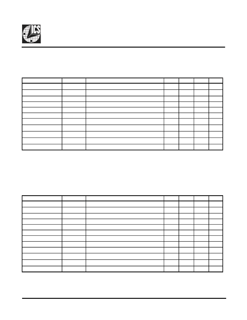
Electrical Characteristics - SDRAM
T
A
= 0 - 70
o
C; V
DD
= 3.3 V +/-5%, V
DDL
= 2.5 V +/-5%; C
L
= 30 pF (unless otherwise stated)
PARAMETER
SYMBOL
Output Impedance
R
DSP2A
V
O
=V
DD
*(0.5)
Output Impedance
R
DSN2A
V
O
=V
DD
*(0.5)
Output High Voltage
V
OH3
I
OH
= -25 mA
Output Low Voltage
V
OL3
I
OL
= 20 mA
Output High Current
I
OH3
V
OH
= 2.0 V
Output Low Current
I
OL3
V
OL
= 0.8 V
Rise Time
T
r3
V
OL
= 0.4 V, V
OH
= 2.4 V
Fall Time
T
f3
V
OH
= 2.4 V, V
OL
= 0.4 V
Duty Cycle
D
t3
V
T
= 1.5 V
Skew
1
(0-1,2,4,5,7,10,11)
T
sk1
V
T
= 1.5 V
Skew
1
(0-6,6,8,9,12,13)
T
sk1
V
T
= 1.5 V
Jitter, Cycle-to-cycle
t
jcyc
V
T
= 1.5 V
1
Guarenteed by design, not 100% tested in production.
CONDITIONS
MIN
10
10
2.4
TYP
17
18
2.9
0.32
-73
50
1.14
1.38
51.8
155.5
298.5
369.17
MAX
20
20
UNITS
V
V
mA
mA
ns
ns
%
ps
ps
ps
1
1
0.4
-40
41
0.4
0.4
47
1
2
2
1
1
57
250
500
650
Electrical Characteristics - PCI
T
A
= 0 - 70C; V
DD
= 3.3 V +/-5%; V
DDL
= 2.5 V +/-5%; C
L
= 30 pF
PARAMETER
SYMBOL
CONDITIONS
MIN
TYP
MAX
UNITS
V
V
mA
mA
ns
ns
%
ps
ps
Output Impedance
Output Impedance
Output High Voltage
Output Low Voltage
Output High Current
Output Low Current
Rise Time
1
Fall Time
1
Duty Cycle
1
Skew
1
Jitter, Cycle-to-cycle
R
DSP1
R
DSP1
V
OH2
V
OL2
I
OH2
I
OL2
t
r2
t
f2
d
t2
t
sk2
t
jcyc2
1
V
O
=V
DD
*(0.5)
V
O
=V
DD
*(0.5)
I
OH
= -18 mA
I
OL
= 9.4 mA
V
OH
= 2.0 V
V
OL
= 0.8 V
V
OL
= 0.4 V, V
OH
= 2.4 V
V
OH
= 2.4 V, V
OL
= 0.4 V
V
T
= 1.5 V
V
T
= 1.5 V
V
T
= 1.5 V
12
12
2.4
21
21
3.3
0.17
-62
43
1.62
1.81
49.8
200
306
55
55
1
0.4
-33
38
2.2
2.2
55
500
350
45
-350
1
Guaranteed by design, not 100% tested in production.
相關(guān)PDF資料 |
PDF描述 |
|---|---|
| ICS9248F-56 | Peripheral IC |
| ICS9248G50 | Industrial Control IC |
| ICS9248YG-50 | Peripheral IC |
| ICS9248YG-50T | Peripheral IC |
| ICS9250F-19 | Peripheral IC |
相關(guān)代理商/技術(shù)參數(shù) |
參數(shù)描述 |
|---|---|
| ICS9248F-151-T | 制造商:ICS 制造商全稱:ICS 功能描述:Frequency Generator & Integrated Buffers for Celeron & PII/III⑩ |
| ICS9248F-163-T | 制造商:ICS 制造商全稱:ICS 功能描述:AMD - K7 System Clock Chip |
| ICS9248F-20 | 制造商:ICS 制造商全稱:ICS 功能描述:Pentium/ProTM System Clock Chip |
| ICS9248F-56 | 制造商:未知廠家 制造商全稱:未知廠家 功能描述:Peripheral IC |
| ICS9248F-61 | 制造商:ICS 制造商全稱:ICS 功能描述:Frequency Timing Generator for Pentium II Systems |
發(fā)布緊急采購,3分鐘左右您將得到回復(fù)。