- 您現(xiàn)在的位置:買賣IC網(wǎng) > PDF目錄360788 > ICSLV810 Buffer/Clock Driver PDF資料下載
參數(shù)資料
| 型號(hào): | ICSLV810 |
| 英文描述: | Buffer/Clock Driver |
| 中文描述: | 緩沖器/時(shí)鐘驅(qū)動(dòng)器 |
| 文件頁數(shù): | 6/12頁 |
| 文件大小: | 145K |
| 代理商: | ICSLV810 |
Buffer/Clock Driver
MDS LV810 F
6
Revision 101305
Integrated Circuit Systems, Inc.
●
525 Race Street, San Jose, CA 95126
●
tel (408) 297-1201
●
www.icst.com
ICSLV810
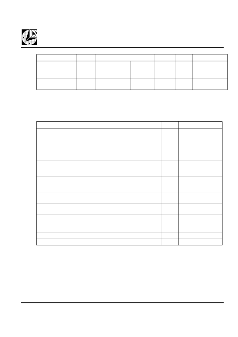
Note1:
This parameter is not tested, guaranteed by design.
AC Electrical Characteristics—Bank A
VDDA = 2.5 V
, Ambient Temperature -40
°
C to +85
°
C
Parameter
Output Skew: skew between
outputs of same package
Input High Current
I
I
VDDC = max,
VIN = VDD (max)
VIN
= 0V, Note1
V
OUT
= 0V,
Note 1
20
μA
Input Capacitance
Output Capacitance
C
IN
C
OUT
5
6.0
8.0
pF
pF
5.5
Symbol
t
SK(0
)
Conditions
CL = 3 pF,
RL = 500
Figure 3
CL = 3 pF,
RL = 500
Figure 4
CL = 3 pF,
RL = 500
Figure 2
CL = 3 pF,
RL = 500
Figure 5
CL = 3 pF,
RL = 500
CL = 3 pF,
RL = 500
All Outputs
CL = 3 pF,
RL = 500
Min.
-200
Typ.
Max.
200
Units
ps
Pulse Skew: skew between
opposite transitions of same
output (t
PLH
-t
PHL
)
Propagation Delay
t
SK(P)
-200
200
ps
t
pLH
/ t
pHL
1.5
2.6
3.5
ns
Part to Part Skew
t
SK(t)
-650
650
ps
Output Rise Time
20% to 80%
Output Fall Time
80% to 20%
Additive Jitter
Duty Cycle
Measured at VDD/2
Duty Cycle, VDDA=1.8V
Output Frequency Range
t
r(o)
0.8
ns
t
f(o)
0.8
ns
t
J
50
55
ps
%
DC
45
DC
40
1
50
60
133
%
MHz
Parameter
Symbol
Conditions
Min.
Typ.
Max.
Units
相關(guān)PDF資料 |
PDF描述 |
|---|---|
| ICSLV810FI | Buffer/Clock Driver |
| ICSLV810FILF | Buffer/Clock Driver |
| ICSLV810FILFT | Buffer/Clock Driver |
| ICSLV810FIT | Buffer/Clock Driver |
| ICSLV810RI | Buffer/Clock Driver |
相關(guān)代理商/技術(shù)參數(shù) |
參數(shù)描述 |
|---|---|
| ICSLV810FI | 制造商:ICS 制造商全稱:ICS 功能描述:Buffer/Clock Driver |
| ICSLV810FILF | 制造商:ICS 制造商全稱:ICS 功能描述:Buffer/Clock Driver |
| ICSLV810FILFT | 制造商:ICS 制造商全稱:ICS 功能描述:Buffer/Clock Driver |
| ICSLV810FIT | 制造商:ICS 制造商全稱:ICS 功能描述:Buffer/Clock Driver |
| ICSLV810RI | 制造商:ICS 制造商全稱:ICS 功能描述:Buffer/Clock Driver |
發(fā)布緊急采購(gòu),3分鐘左右您將得到回復(fù)。