- 您現(xiàn)在的位置:買賣IC網(wǎng) > PDF目錄377165 > IDT54FCT16827BTPVB (Integrated Device Technology, Inc.) 400MHz Clock Generator for Server/Workstation PDF資料下載
參數(shù)資料
| 型號(hào): | IDT54FCT16827BTPVB |
| 廠商: | Integrated Device Technology, Inc. |
| 英文描述: | 400MHz Clock Generator for Server/Workstation |
| 中文描述: | 快速CMOS 20位緩沖器 |
| 文件頁(yè)數(shù): | 1/8頁(yè) |
| 文件大小: | 120K |
| 代理商: | IDT54FCT16827BTPVB |
Integrated Device Technology, Inc.
DESCRIPTION:
The FCT16827AT/BT/CT/ET and FCT162827AT/BT/CT/
ET 20-bit buffers are built using advanced dual metal CMOS
technology. These 20-bit bus drivers provide high-perfor-
mance bus interface buffering for wide data/address paths or
busses carrying parity. Two pair of NAND-ed output enable
controls offer maximum control flexibility and are organized to
operate the device as two 10-bit buffers or one 20-bit buffer.
Flow-through organization of signal pins simplifies layout. All
inputs are designed with hysteresis for improved noise mar-
gin.
The FCT16827AT/BT/CT/ET are ideally suited for driving
high capacitance loads and low impedance backplanes. The
output buffers are designed with power off disable capability
to allow "live insertion" of boards when used as backplane
drivers.
The FCT162827AT/BT/CT/ET have balanced output drive
with current limiting resistors. This offers low ground bounce,
minimal undershoot, and controlled output fall times–reducing
the need for external series terminating resistors. The
FCT162827AT/BT/CT/ET are plug-in replacements for the
FCT16827AT/BT/CT/ET and ABT16827 for on-board inter-
face applications.
FAST CMOS 20-BIT
BUFFERS
IDT54/74FCT16827AT/BT/CT/ET
IDT54/74FCT162827AT/BT/CT/ET
FEATURES:
Common features:
–
0.5 MICRON CMOS Technology
–
High-speed, low-power CMOS replacement for
ABT functions
–
Typical t
SK
(o) (Output Skew) < 250ps
–
Low input and output leakage
≤
1
μ
A (max.)
–
ESD > 2000V per MIL-STD-883, Method 3015;
> 200V using machine model (C = 200pF, R = 0)
–
Packages include 25 mil pitch SSOP, 19.6 mil pitch
TSSOP, 15.7 mil pitch TVSOP and 25 mil pitch Cerpack
–
Extended commercial range of -40
°
C to +85
°
C
–
V
CC
= 5V
±
10%
Features for FCT16827AT/BT/CT/ET:
–
High drive outputs (-32mA I
OH
, 64mA I
OL
)
–
Power off disable outputs permit “l(fā)ive insertion”
–
Typical V
OLP
(Output Ground Bounce) < 1.0V at
V
CC
= 5V, T
A
= 25
°
C
Features for FCT162827AT/BT/CT/ET:
–
Balanced Output Drivers:
±
24mA (commercial),
±
16mA (military)
–
–
Reduced system switching noise
Typical V
OLP
(Output Ground Bounce) < 0.6V at
V
CC
= 5V,T
A
= 25
°
C
The IDT logo is a registered trademark of Integrated Device Technology, Inc.
MILITARY AND COMMERCIAL TEMPERATURE RANGES
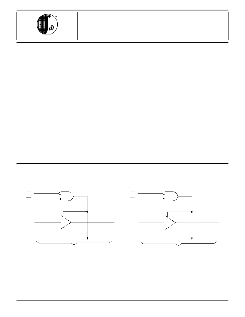
1
Y
1
TO 9 OTHER CHANNELS
1
OE
1
1
OE
2
1
A
1
2773 drw 01
2773 drw 02
AUGUST 1996
1996 Integrated Device Technology, Inc.
5.17
DSC-2773/7
1
FUNCTIONAL BLOCK DIAGRAM
2
Y
1
TO 9 OTHER CHANNELS
2
OE
1
2
OE
2
2
A
1
相關(guān)PDF資料 |
PDF描述 |
|---|---|
| IDT74FCT16827BTPVB | FAST CMOS 20-BIT BUFFERS |
| IDT54FCT162827BTPVB | FAST CMOS 20-BIT BUFFERS |
| IDT74FCT162827BTPVB | 400MHz Clock Generator for Mobile PC |
| IDT54FCT16827AT | FAST CMOS 20-BIT BUFFERS |
| IDT54FCT16827ATE | FAST CMOS 20-BIT BUFFERS |
相關(guān)代理商/技術(shù)參數(shù) |
參數(shù)描述 |
|---|---|
| IDT54FCT191DB | 制造商:Integrated Device Technology Inc 功能描述: |
| IDT54FCT2374KATEB | 制造商:Rochester Electronics LLC 功能描述:- Bulk |
| IDT54FCT240ATDB | 制造商:Integrated Device Technology Inc 功能描述:IC TXRX 16BIT BIDIRECT 20CERPACK |
| IDT54FCT240ATLB | 制造商:Integrated Device Technology Inc 功能描述: 制造商:Integrated Device Technology Inc 功能描述:IC TXRX 16BIT BIDIRECT 20LCC |
| IDT54FCT240CTDB | 制造商:Integrated Device Technology Inc 功能描述:IC TXRX 16BIT BIDIRECT 20CERDIP |
發(fā)布緊急采購(gòu),3分鐘左右您將得到回復(fù)。