- 您現(xiàn)在的位置:買賣IC網(wǎng) > PDF目錄377193 > IDT54FCT2543DTPB (Integrated Device Technology, Inc.) FAST CMOS OCTAL LATCHED TRANSCEIVER PDF資料下載
參數(shù)資料
| 型號(hào): | IDT54FCT2543DTPB |
| 廠商: | Integrated Device Technology, Inc. |
| 英文描述: | FAST CMOS OCTAL LATCHED TRANSCEIVER |
| 中文描述: | 快速CMOS八進(jìn)制鎖存收發(fā)器 |
| 文件頁(yè)數(shù): | 2/7頁(yè) |
| 文件大?。?/td> | 119K |
| 代理商: | IDT54FCT2543DTPB |
IDT54/74FCT543T/AT/CT/DT - 2543T/AT/CT
FAST CMOS OCTAL LATCHED TRANSCEIVER
MILITARY AND COMMERCIAL TEMPERATURE RANGES
6.17
2
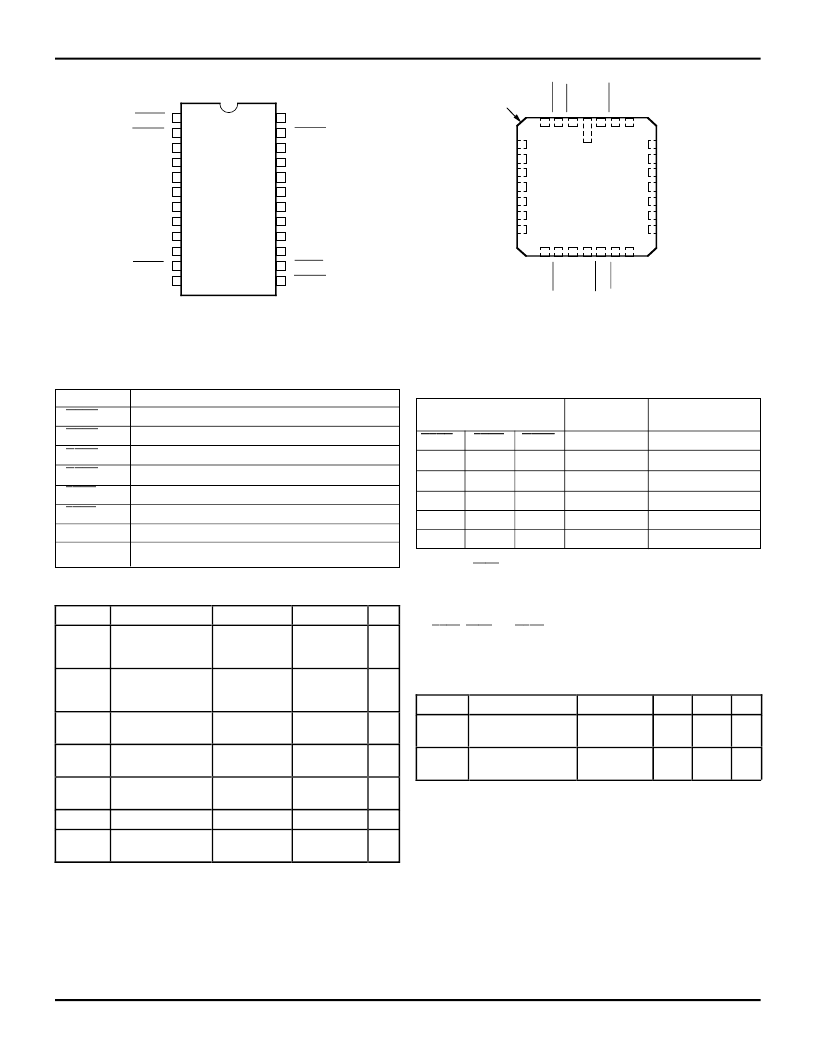
PIN CONFIGURATIONS
DIP/SOIC/SSOP/QSOP/CERPACK
TOP VIEW
5
6
7
8
9
10
11
12
GND
A
0
A
1
A
2
A
3
A
4
A
5
A
6
A
7
1
2
3
4
24
23
22
21
20
19
18
17
16
15
14
13
Vcc
CEBA
P24-1
D24-1
SO24-2
SO24-7
SO24-8
&
E24-1
B
0
B
1
B
2
B
3
B
4
B
5
B
6
B
7
LEAB
OEAB
LEBA
OEBA
CEAB
LCC
TOP VIEW
5
6
7
8
9
10
11
L28-1
25
24
23
22
21
20
19
INDEX
A
1
A
2
A
3
NC
A
4
A
5
A
6
N
V
G
N
NC
B
4
B
5
B
6
B
1
B
2
B
3
A
0
L
O
B
0
C
A
7
C
B
7
L
O
12 13 14 15 16 17 18
4
3
2
1
28 27 26
2613 drw 02
2613 drw 03
FUNCTION TABLE
(1, 2)
For A-to-B (Symmetric with B-to-A)
Latch
Status
A-to-B
Storing
Storing
Output
Buffers
B
0
–B
7
Inputs
LEAB
CEAB
OEAB
H
—
—
L
L
—
H
—
L
H
—
—
H
L
L
High Z
—
—
High Z
Current A Inputs
Previous* A Inputs
Transparent
Storing
NOTES:
1. * Before
LEAB
LOW-to-HIGH Transition
H = HIGH Voltage Level
L = LOW Voltage Level
— = Don’t Care or Irrelevant
2. A-to-B data flow shown; B-to-A flow control is the same, except using
CEBA
,
LEBA
and
OEBA
.
2613 tbl 02
ABSOLUTE MAXIMUM RATINGS
(1)
Symbol
Rating
V
TERM(2)
Terminal Voltage
with Respect to
GND
V
TERM(3)
Terminal Voltage
with Respect to
GND
T
A
Operating
Temperature
T
BIAS
Temperature
Under Bias
T
STG
Storage
Temperature
P
T
Power Dissipation
Commercial
–0.5 to +7.0
Military
–0.5 to +7.0
Unit
V
–0.5 to
V
CC
+0.5
–0.5 to
V
CC
+0.5
V
0 to +70
–55 to +125
°
C
–55 to +125
–65 to +135
°
C
–55 to +125
–65 to +150
°
C
0.5
0.5
W
I
OUT
DC Output
Current
–60 to +120 –60 to +120 mA
NOTES:
1. Stresses greater than those listed under ABSOLUTE MAXIMUM RAT-
INGS may cause permanent damage to the device. This is a stress rating
only and functional operation of the device at these or any other conditions
above those indicated in the operational sections of this specification is
not
implied. Exposure to absolute maximum rating conditions for
extended periods may affect reliability. No terminal voltage may exceed
V
CC
by +0.5V unless otherwise noted.
2. Input and V
CC
terminals only.
3. Outputs and I/O terminals only.
2613 lnk 03
PIN DESCRIPTION
Pin Names
OEAB
Description
A-to-B Output Enable Input (Active LOW)
B-to-A Output Enable Input (Active LOW)
A-to-B Enable Input (Active LOW)
B-to-A Enable Input (Active LOW)
A-to-B Latch Enable Input (Active LOW)
B-to-A Latch Enable Input (Active LOW)
A-to-B Data Inputs or B-to-A 3-State Outputs
B-to-A Data Inputs or A-to-B 3-State Outputs
OEBA
CEAB
CEBA
LEAB
LEBA
A
0
–A
7
B
0
–B
7
2613 tbl 01
CAPACITANCE
(T
A
= +25
°
C, f = 1.0MHz)
Symbol
C
IN
Parameter
(1)
Input
Capacitance
Output
Capacitance
Conditions
V
IN
= 0V
Typ.
6
Max. Unit
10
pF
C
OUT
V
OUT
= 0V
8
12
pF
NOTE:
1. This parameter is measured at characterization but not tested.
2613 lnk 04
相關(guān)PDF資料 |
PDF描述 |
|---|---|
| IDT54FCT2543DTPY | FAST CMOS OCTAL LATCHED TRANSCEIVER |
| IDT54FCT2543DTPYB | CAP 4700PF 25V 10% X7R SMD-1206 TR-7-PL SN-NIBAR |
| IDT74FCT2543ATSOB | FAST CMOS OCTAL LATCHED TRANSCEIVER |
| IDT74FCT2543CT | FAST CMOS OCTAL LATCHED TRANSCEIVER |
| IDT74FCT2543CTD | FAST CMOS OCTAL LATCHED TRANSCEIVER |
相關(guān)代理商/技術(shù)參數(shù) |
參數(shù)描述 |
|---|---|
| IDT54FCT273DB | 制造商:Integrated Device Technology Inc 功能描述: |
| IDT54FCT273TDB | 制造商:Integrated Device Technology Inc 功能描述:Flip Flop D-Type Bus Interface Pos-Edge 1-Element 20-Pin CDIP |
| IDT54FCT273TLB | 制造商:Integrated Device Technology Inc 功能描述:Flip Flop D-Type Bus Interface Pos-Edge 1-Element 20-Pin LCC |
| IDT54FCT299ADB | 制造商:Integrated Device Technology Inc 功能描述: |
| IDT54FCT299DB | 制造商:Integrated Device Technology Inc 功能描述:Shift Register, 20 Pin, Ceramic, DIP |
發(fā)布緊急采購(gòu),3分鐘左右您將得到回復(fù)。