- 您現(xiàn)在的位置:買賣IC網(wǎng) > PDF目錄377217 > IDT54FCT810BTEB (INTEGRATED DEVICE TECHNOLOGY INC) FAST CMOS BUFFER/CLOCK DRIVER PDF資料下載
參數(shù)資料
| 型號: | IDT54FCT810BTEB |
| 廠商: | INTEGRATED DEVICE TECHNOLOGY INC |
| 元件分類: | 時鐘及定時 |
| 英文描述: | FAST CMOS BUFFER/CLOCK DRIVER |
| 中文描述: | FCT SERIES, LOW SKEW CLOCK DRIVER, 5 TRUE OUTPUT(S), 5 INVERTED OUTPUT(S), CDFP20 |
| 封裝: | CERPACK-20 |
| 文件頁數(shù): | 2/6頁 |
| 文件大?。?/td> | 107K |
| 代理商: | IDT54FCT810BTEB |
IDT54/74FCT810BT/CT
FAST CMOS BUFFER/CLOCK DRIVER
MILITARY AND COMMERCIAL TEMPERATURE RANGES
9.4
2
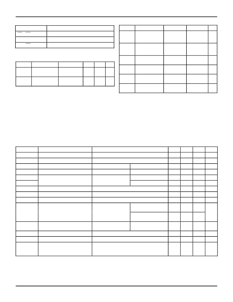
PIN DESCRIPTION
3103 tbl 01
CAPACITANCE
(T
A
= +25
°
C, f = 1.0MHz)
Symbol
Parameter
(1)
C
IN
Input
Capacitance
C
OUT
Output
Capacitance
NOTE:
1. This parameter is measured at characterization but not tested.
Conditions
V
IN
= 0V
Typ.
4.5
Max.
6.0
Unit
pF
V
OUT
= 0V
5.5
8.0
pF
ABSOLUTE MAXIMUM RATINGS
(1)
Symbol
Rating
V
TERM(2)
Terminal Voltage
with Respect to
GND
V
TERM(3)
Terminal Voltage
with Respect to
GND
T
A
Operating
Temperature
T
BIAS
Temperature
Under Bias
T
STG
Storage
Temperature
I
OUT
DC Output
Current
NOTES:
1. Stresses greater than those listed under ABSOLUTE MAXIMUM RAT-
INGS may cause permanent damage to the device. This is a stress rating
only and functional operation of the device at these or any other conditions
above those indicated in the operational sections of this specification is
not
implied. Exposure to absolute maximum rating conditions for
extended periods may affect reliability. No terminal voltage may exceed
V
CC
by +0.5V unless otherwise noted.
2. Input and V
CC
terminals.
3. Output and I/O terminals.
Commercial
–0.5 to +7.0
Military
–0.5 to +7.0
Unit
V
–0.5 to V
CC
+0.5
–0.5 to V
CC
+0.5
V
0 to +70
–55 to +125
°
C
–55 to +125
–65 to +135
°
C
–55 to +125
–65 to +150
°
C
–60 to +120
–60 to +120
mA
3103 lnk 03
DC ELECTRICAL CHARACTERISTICS OVER OPERATING RANGE
Following Conditions Apply Unless Otherwise Specified
Commercial: T
A
= 0
°
C to +70
°
C, V
CC
= 5.0V
±
5%; Military: T
A
= –55
°
C to +125
°
C, V
CC
= 5.0V
±
10%
Symbol
Parameter
V
IH
Input HIGH Level
Guaranteed Logic HIGH Level
NOTES:
1. For conditions shown as Max. or Min., use appropriate value specified under Electrical Characteristics for the applicable device type.
2. Typical values are at Vcc = 5.0V, +25
°
C ambient.
3. Not more than one output should be tested at one time. Duration of the test should not exceed one second.
4. Duration of the condition can not exceed one second.
5. The test limit for this parameter is
±
5
μ
A at T
A
= –55
°
C.
Test Conditions
(1)
Min.
2.0
Typ.
(2)
—
Max.
—
Unit
V
V
IL
I
I H
I
I L
Input LOW Level
Input HIGH Current
(5)
Input LOW Current
(5)
Guaranteed Logic LOW Level
V
CC
= Max.
V
CC
= Max.
—
—
—
—
—
—
0.8
±
1
±
1
±
1
±
1
±
1
–1.2
–225
—
V
μ
A
μ
A
μ
A
μ
A
μ
A
V
mA
V
V
I
= 2.7V
V
I
= 0.5V
I
OZH
I
OZL
I
I
High Impedance Output Current
(3-State Output pins)
(5)
Input HIGH Current
(5)
V
CC
= Max.
V
O
= 2.7V
V
O
= 0.5V
—
—
—
—
—
—
V
CC
= Max., V
I
= V
CC
(Max.)
V
IK
I
OS
V
OH
Clamp Diode Voltage
Short Circuit Current
Output HIGH Voltage
V
CC
= Min., I
IN
= –18mA
V
CC
= Max.
(3)
, V
O
= GND
V
CC
= Min.
V
IN
= V
IH
or V
IL
—
–60
2.4
–0.7
–120
3.3
I
OH
= –12mA MIL.
I
OH
= –15mA COM'L.
I
OH
= –24mA MIL.
I
OH
= –32mA COM'L.
(4)
I
OL
= 32mA MIL.
I
OL
= 48mA COM'L.
2.0
3.0
—
V
OL
Output LOW Voltage
V
CC
= Min.
V
IN
= V
IH
or V
IL
V
CC
= 0V, V
IN
or V
O
≤
4.5V
—
0.3
0.55
V
I
OFF
Input/Output Power Off Leakage
(5)
Input Hysteresis for all inputs
—
—
—
150
±
1
—
μ
A
mV
μ
A
V
H
—
I
CCL
I
CCH
I
CCZ
Quiescent Power Supply Current
V
CC
= Max., V
IN
= GND or V
CC
—
5
500
3103 lnk 04
3103 lnk 02
Pin Names
OE
A
,
OE
B
IN
A
, IN
B
OA
n
,
OB
n
Description
3-State Output Enable Inputs (Active LOW)
Clock Inputs
Clock Outputs
相關(guān)PDF資料 |
PDF描述 |
|---|---|
| IDT54FCT810BTL | FAST CMOS BUFFER/CLOCK DRIVER |
| IDT54FCT810BTLB | FAST CMOS BUFFER/CLOCK DRIVER |
| IDT54FCT810BTP | FAST CMOS BUFFER/CLOCK DRIVER |
| IDT54FCT810BTPB | FAST CMOS BUFFER/CLOCK DRIVER |
| IDT54FCT810BTPY | FAST CMOS BUFFER/CLOCK DRIVER |
相關(guān)代理商/技術(shù)參數(shù) |
參數(shù)描述 |
|---|---|
| IDT54FCT821ADB | 制造商:Integrated Device Technology Inc 功能描述: |
| IDT54FCT821BDB | 制造商:Integrated Device Technology Inc 功能描述: |
| IDT54FCT821HATEB | 制造商:Integrated Device Technology Inc 功能描述: |
| IDT54FCT821HCTEB | 制造商:Rochester Electronics LLC 功能描述:- Bulk |
| IDT54FCT845ADB | 制造商:Integrated Device Technology Inc 功能描述: |
發(fā)布緊急采購,3分鐘左右您將得到回復(fù)。