- 您現(xiàn)在的位置:買賣IC網(wǎng) > PDF目錄65576 > IDT5993A-2Q8 (INTEGRATED DEVICE TECHNOLOGY INC) PLL BASED CLOCK DRIVER, 8 TRUE OUTPUT(S), 0 INVERTED OUTPUT(S), PDSO28 PDF資料下載
參數(shù)資料
| 型號(hào): | IDT5993A-2Q8 |
| 廠商: | INTEGRATED DEVICE TECHNOLOGY INC |
| 元件分類: | 時(shí)鐘及定時(shí) |
| 英文描述: | PLL BASED CLOCK DRIVER, 8 TRUE OUTPUT(S), 0 INVERTED OUTPUT(S), PDSO28 |
| 封裝: | QSOP-28 |
| 文件頁(yè)數(shù): | 2/8頁(yè) |
| 文件大小: | 65K |
| 代理商: | IDT5993A-2Q8 |
2
COMMERCIALANDINDUSTRIALTEMPERATURERANGES
IDT5993A
PROGRAMMABLESKEWPLLCLOCKDRIVERTURBOCLOCK
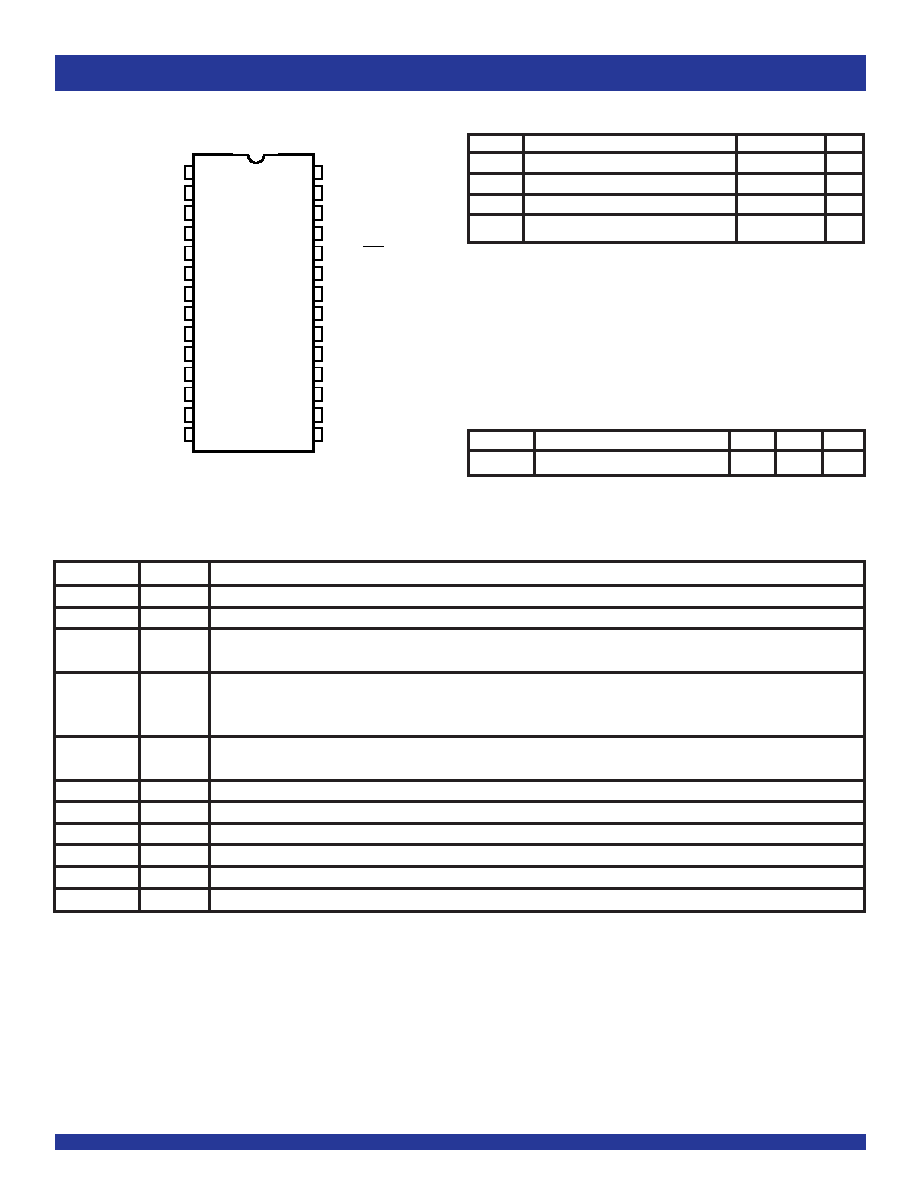
PIN CONFIGURATION
NOTE:
1. Stresses beyond those listed under ABSOLUTE MAXIMUM RATINGS may cause
permanent damage to the device. These are stress ratings only, and functional
operation of the device at these or any other conditions above those indicated in the
operational sections of this specification is not implied. Exposure to absolute-
maximum-rated conditions for extended periods may affect device reliability.
ABSOLUTE MAXIMUM RATINGS(1)
Symbol
Description
Max
Unit
Supply Voltage to Ground
–0.5 to +7
V
VI
DC Input Voltage
–0.5 to +7
V
Maximum Power Dissipation (TA = 85°C)
0.66
W
TSTG
Storage Temperature
–65 to +150
°C
NOTE:
1. Capacitance applies to all inputs except TEST, FS, and nF1:0. It is characterized but
not production tested.
CAPACITANCE(TA=+25°C,f=1MHz,VIN=0V)
Parameter
Description
Typ.
Max.
Unit
CIN
InputCapacitance
4
6
pF
QSOP
TOP VIEW
Output skew with respect to the REF input is adjustable to compensate
for PCB trace delays, backplane propagation delays or to accommodate
requirements for special timing relationships between clocked compo-
nents. Skew is selectable as a multiple of a time unit tU which is of the
order of a nanosecond (see PLL Programmable Skew Range and Resolution
Table). There are nine skew configurations available for each output
pair. These configurations are chosen by the nF1:0 control pins. In order
to minimize the number of control pins, 3-level inputs (HIGH-MID-LOW)
are used, they are intended for but not restricted to hard-wiring. Undriven
3-level inputs default to the MID level. Where programmable skew is
not a requirement, the control pins can be left open for the zero skew
default setting. The Control Summary Table shows how to select specific
skew taps by using the nF1:0 control pins.
PROGRAMMABLESKEW
PIN DESCRIPTION
Pin Name
Type
Description
REF
IN
ReferenceClockInput
FB
IN
FeedbackInput
TEST(1)
IN
When MID or HIGH, disables PLL (except for conditions of Note 1). REF goes to all outputs. Skew Selections (See Control
SummaryTable)remainineffect. SetLOWfornormaloperation.
GND/ sOE(1)
IN
Synchronous Output Enable. When HIGH, it stops clock outputs (except 3Q0 and 3Q1) in a LOW state - 3Q0 and 3Q1may be used as
thefeedbacksignaltomaintainphaselock. WhenTESTisheldatMIDlevelandGND/sOE isHIGH,thenF[1:0]pinsactasoutputdisable
controls for individual banks when nF[1:0] = LL. Set GND/sOE LOW for normal operation.
VCCQ/PE
IN
Selectablepositiveornegativeedgecontrol. WhenLOW/HIGHtheoutputsaresynchronizedwiththenegative/positiveedge ofthe
referenceclock.
nF[1:0]
IN
3-level inputs for selecting 1 of 9 skew taps or frequency functions
FS
IN
Selectsappropriateoscillatorcirciotbasedonanticipatedfrequencyrange. (SeePLLProgrammableSkewRange.)
nQ[1:0]
OUT
Three output banks of two outputs with programmable skew (1Q:3Q), and 4Q output has fixed zero skew outputs.
VCCN
PWR
Powersupplyforoutputbuffers
VCCQ
PWR
Powersupplyforphase lockedloop and other internal circuitry
GND
PWR
Ground
NOTE:
1. When TEST = MID and GND/sOE = HIGH, PLL remains active with nF[1:0] = LL functioning as an output disable control for individual output banks. Skew selections remain
in effect unless nF[1:0] = LL.
1
2
3
4
5
6
7
8
9
10
11
12
13
14
28
27
26
25
24
23
22
21
20
19
18
17
16
15
REF
FS
3F0
3F1
4Q1
4Q0
GND
3Q1
3Q0
FB
GND
TEST
2F1
2F0
GND/sOE
1F1
1F0
VCCN
1Q0
1Q1
GND
2Q0
2Q1
VCCN
VCCQ/PE
VCCQ
相關(guān)PDF資料 |
PDF描述 |
|---|---|
| IDT5993A-7QI8 | PLL BASED CLOCK DRIVER, 8 TRUE OUTPUT(S), 0 INVERTED OUTPUT(S), PDSO28 |
| IDT5T9070PAGI | 5T SERIES, LOW SKEW CLOCK DRIVER, 10 TRUE OUTPUT(S), 0 INVERTED OUTPUT(S), PDSO48 |
| IDT5T9950APFGI | 5T SERIES, PLL BASED CLOCK DRIVER, 8 TRUE OUTPUT(S), 0 INVERTED OUTPUT(S), PQFP32 |
| IDT5T9950APFGI8 | 5T SERIES, PLL BASED CLOCK DRIVER, 8 TRUE OUTPUT(S), 0 INVERTED OUTPUT(S), PQFP32 |
| IDT5T9950PFI | 5T SERIES, PLL BASED CLOCK DRIVER, 8 TRUE OUTPUT(S), 0 INVERTED OUTPUT(S), PQFP32 |
相關(guān)代理商/技術(shù)參數(shù) |
參數(shù)描述 |
|---|---|
| IDT5P30017NDGI | 制造商:Integrated Device Technology Inc 功能描述:IC CLOCK GENERATOR 28QFN |
| IDT5P30017NDGI8 | 制造商:Integrated Device Technology Inc 功能描述:IC CLOCK GENERATOR 28QFN |
| IDT5P30018NBG8 | 制造商:Integrated Device Technology Inc 功能描述:IC CLOCK GENERATOR 28QFN |
| IDT5P49EE502NDGI | 制造商:Integrated Device Technology Inc 功能描述:IC CLOCK GENERATOR 20QFN |
| IDT5P49EE502NDGI8 | 制造商:Integrated Device Technology Inc 功能描述:IC CLOCK GENERATOR 28QFN |
發(fā)布緊急采購(gòu),3分鐘左右您將得到回復(fù)。