- 您現(xiàn)在的位置:買賣IC網(wǎng) > PDF目錄377248 > IDT6167LA85PB (Integrated Device Technology, Inc.) CMOS STATIC RAM 16K (16K x 1-BIT) PDF資料下載
參數(shù)資料
| 型號: | IDT6167LA85PB |
| 廠商: | Integrated Device Technology, Inc. |
| 英文描述: | CMOS STATIC RAM 16K (16K x 1-BIT) |
| 中文描述: | 16K的的CMOS靜態(tài)RAM(16K的× 1位) |
| 文件頁數(shù): | 5/8頁 |
| 文件大小: | 63K |
| 代理商: | IDT6167LA85PB |
5.2
5
IDT6167SA/LA
CMOS STATIC RAM 16K (16K x 1-BIT)
MILITARY AND COMMERCIAL TEMPERATURE RANGES
AC TEST CONDITIONS
Input Pulse Levels
GND to 3.0V
Input Rise/Fall Times
5ns
Input Timing Reference Levels
1.5V
Output Reference Levels
1.5V
AC Test Load
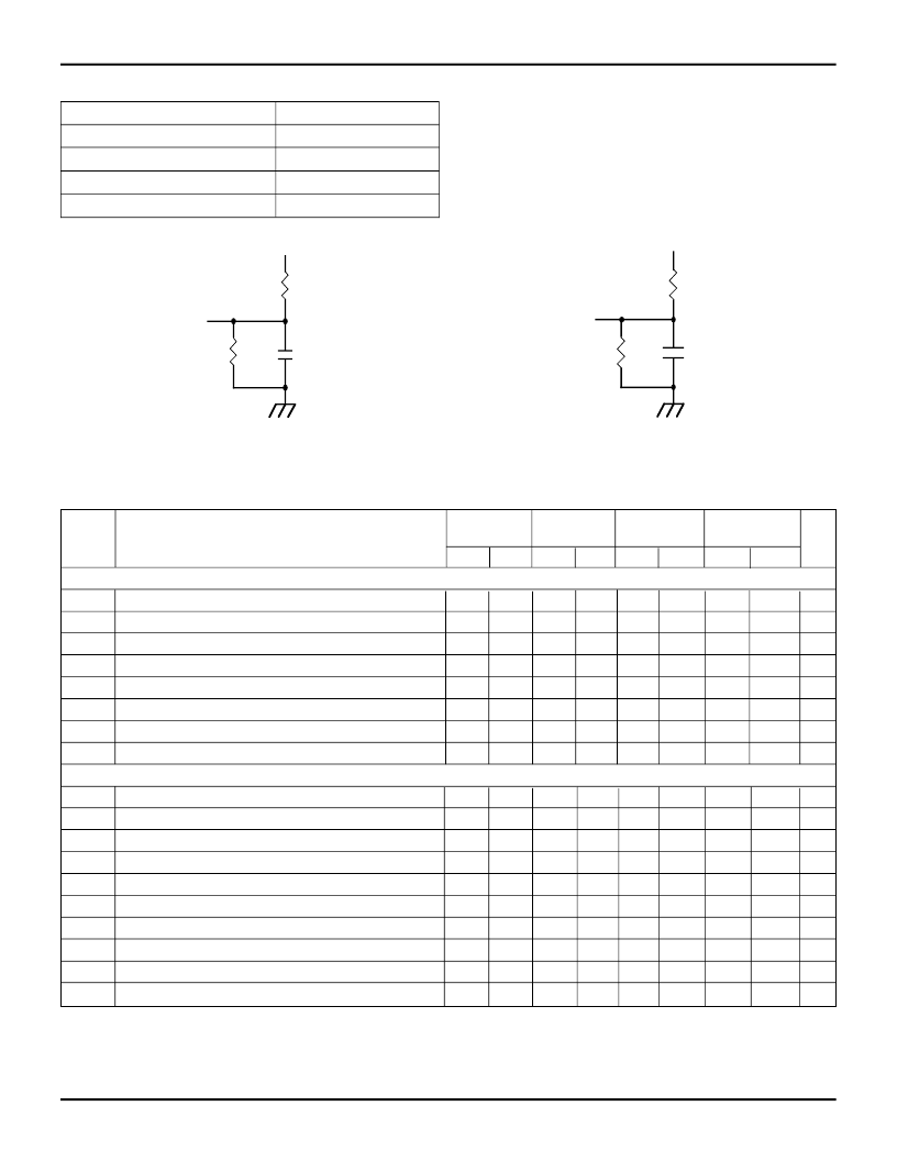
See Figures 1 and 2
2981 tbl 10
Figure 2. AC Test Load
(for t
CLZ
, t
CHZ
, t
WHZ
and t
OW
)
*Includes scope and jig.
Figure 1. AC Test Load
2981 drw 04
480
30pF*
255
DATA
OUT
5V
2981 drw 05
480
5pF*
255
DATA
OUT
5V
AC ELECTRICAL CHARACTERISTICS
(V
CC
= 5.0V
±
10%, All Temperature Ranges)
6167SA15
6167LA15
Min.
6167SA20/25 6167SA35/45
(1)
6167SA55
(1)
/70
(1)
6167LA20/25 6167LA35/45
(1)
6167LA55
(1)
/70
(1)
Min.
Max.
Min.
Max.
Symbol
Parameter
Max.
Min.
Max.
Unit
Read Cycle
t
RC
Read Cycle Time
15
—
20/25
—
35/45
—
55/70
—
ns
t
AA
Address Access Time
—
15
—
20/25
—
35/45
—
55/70
ns
t
ACS
t
CLZ(2)
t
CHZ(2)
Chip Select Access Time
—
15
—
20/25
—
35/45
—
55/70
ns
Chip Deselect to Output in Low-Z
3
—
5/5
—
5/5
—
5/5
—
ns
Chip Select to Output in High-Z
—
10
—
10/10
—
15/30
—
40/40
ns
t
OH
t
PU(2)
t
PD(2)
Output Hold from Address Change
3
—
5/5
—
5/5
—
5/5
—
ns
Chip Select to Power-Up Time
0
—
0/0
—
0/0
—
0/0
—
ns
Chip Deselect to Power-Down Time
—
15
—
20/25
—
35/45
—
55/70
ns
Write Cycle
t
WC
Write Cycle Time
15
—
20/20
—
30/45
—
55/70
—
ns
t
CW
Chip Select to End-of-Write
15
—
15/20
—
30/40
—
45/55
—
ns
t
AW
Address Valid to End-of-Write
15
—
15/20
—
30/40
—
45/55
—
ns
t
AS
Address Set-up Time
0
—
0/0
—
0/0
—
0/0
—
ns
t
WP
Write Pulse Width
13
—
15/20
—
30/30
—
35/40
—
ns
t
WR
Write Recovery Time
0
—
0/0
—
0/0
—
0/0
—
ns
t
DW
Data Valid to End-of-Write
10
—
12/15
—
17/20
—
25/30
—
ns
t
DH
t
WHZ(2)
t
OW(2)
Data Hold Time
0
—
0/0
—
0/0
—
0/0
—
ns
Write Enable to Output in High-Z
—
7
—
8/8
—
15/30
—
40/40
ns
Output Active from End-of-Write
0
—
0/0
—
0/0
—
0/0
—
ns
NOTES:
1. –55
°
C to +125
°
C temperature range only. Also available: 85ns and 100ns Military devices.
2. This parameter is guaranteed with AC Load (Figure 2) by device characterization, but is not production tested.
2981 tbl 11
相關(guān)PDF資料 |
PDF描述 |
|---|---|
| IDT6168SA15SOB | CMOS STATIC RAM 16K (4K x 4-BIT) |
| IDT6168LA15SOB | CMOS STATIC RAM 16K (4K x 4-BIT) |
| IDT6168SA25SOB | CMOS STATIC RAM 16K (4K x 4-BIT) |
| IDT6168LA25SOB | CMOS STATIC RAM 16K (4K x 4-BIT) |
| IDT6168SA35SOB | CMOS STATIC RAM 16K (4K x 4-BIT) |
相關(guān)代理商/技術(shù)參數(shù) |
參數(shù)描述 |
|---|---|
| IDT6167LA85Y | 制造商:IDT 制造商全稱:Integrated Device Technology 功能描述:CMOS STATIC RAM 16K (16K x 1-BIT) |
| IDT6167LA85YB | 制造商:IDT 制造商全稱:Integrated Device Technology 功能描述:CMOS STATIC RAM 16K (16K x 1-BIT) |
| IDT6167LAE | 制造商:未知廠家 制造商全稱:未知廠家 功能描述:x1 SRAM |
| IDT6167LAF | 制造商:未知廠家 制造商全稱:未知廠家 功能描述:x1 SRAM |
| IDT6167LART | 制造商:未知廠家 制造商全稱:未知廠家 功能描述:x1 SRAM |
發(fā)布緊急采購,3分鐘左右您將得到回復(fù)。