- 您現(xiàn)在的位置:買賣IC網(wǎng) > PDF目錄353732 > IDT7005L70J (Integrated Device Technology, Inc.) HIGH-SPEED 8K x 8 DUAL-PORT STATIC RAM PDF資料下載
參數(shù)資料
| 型號: | IDT7005L70J |
| 廠商: | Integrated Device Technology, Inc. |
| 英文描述: | HIGH-SPEED 8K x 8 DUAL-PORT STATIC RAM |
| 中文描述: | 高速8K的× 8雙端口靜態(tài)RAM |
| 文件頁數(shù): | 15/20頁 |
| 文件大小: | 265K |
| 代理商: | IDT7005L70J |
6.06
4
IDT7005S/L
HIGH-SPEED 8K x 8 DUAL-PORT STATIC RAM
MILITARY AND COMMERCIAL TEMPERATURE RANGES
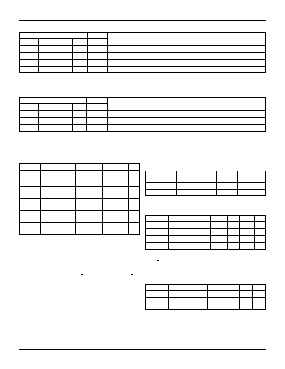
TRUTH TABLE I – NON-CONTENTION READ/WRITE CONTROL
Inputs
(1)
Outputs
CE
R/
W
OE
SEM
I/O0-7
Mode
H
X
H
High-Z
Deselected: Power-Down
L
X
H
DATAIN
Write to Memory
L
H
L
H
DATAOUT
Read Memory
X
H
X
High-Z
Outputs Disabled
NOTE:
2738 tbl 02
1. A0L — A12L is not equal to A0R — A12R.
RECOMMENDED DC OPERATING
CONDITIONS
Symbol
Parameter
Min.
Typ.
Max. Unit
VCC
Supply Voltage
4.5
5.0
5.5
V
GND
Supply Voltage
0
V
VIH
Input High Voltage
2.2
—
6.0
(2)
V
VIL
Input Low Voltage
–0.5
(1)
—
0.8
V
NOTES:
2738 tbl 06
1. VIL > -1.5V for pulse width less than 10ns.
2. VTERM must not exceed Vcc + 0.5V.
RECOMMENDED OPERATING
TEMPERATURE AND SUPPLY VOLTAGE
Ambient
Grade
Temperature
GND
VCC
Military
–55
°C to +125°C
0V
5.0V
± 10%
Commercial
0
°C to +70°C
0V
5.0V
± 10%
2738 tbl 05
ABSOLUTE MAXIMUM RATINGS(1)
Symbol
Rating
Commercial
Military
Unit
VTERM
(2)
Terminal Voltage –0.5 to +7.0
–0.5 to +7.0
V
with Respect
to GND
TA
Operating
0 to +70
–55 to +125
°C
Temperature
TBIAS
Temperature
–55 to +125
–65 to +135
°C
Under Bias
TSTG
Storage
–55 to +125
–65 to +150
°C
Temperature
IOUT
DC Output
50
mA
Current
NOTES:
2738 tbl 04
1. Stresses greater than those listed under ABSOLUTE MAXIMUM
RATINGS may cause permanent damage to the device. This is a stress
rating only and functional operation of the device at these or any other
conditions above those indicated in the operational sections of this
specification is not implied.
Exposure to absolute maximum rating
conditions for extended periods may affect reliability.
2. VTERM must not exceed Vcc + 0.5V for more than 25% of the cycle time
or 10% maximum, and is limited to < 20mA for the period of VTERM > Vcc
+ 0.5V.
CAPACITANCE(1)
(TA = +25
°C, f = 1.0MHz) TQFP PACKAGE
Symbol
Parameter
Conditions
(2)
Max.
Unit
CIN
Input Capacitance
VIN = 3dV
9
pF
COUT
Output
VOUT = 3dV
10
pF
Capacitance
NOTES:
2738 tbl 07
1. This parameter is determined by device characterization but is not
production tested.
2. 3dv references the interpolated capacitance when the input and output
signals switch from 0V to 3V or from 3V to 0V.
TRUTH TABLE II – SEMAPHORE READ/WRITE CONTROL(1)
Inputs
Outputs
CE
R/
W
OE
SEM
I/O0-7
Mode
H
L
DATAOUT
Read in Semaphore Flag Data 0ut
H
u
X
L
DATAIN
Write I/O0 into Semaphore Flag
L
X
L
—
Not Allowed
2738 tbl 03
NOTE:
1. There are eight semaphore flags written to via I/O0 and read from I/O0 - I/O15. These eight semaphores are addressed by A0 - A2.
相關(guān)PDF資料 |
PDF描述 |
|---|---|
| IDT7005L70JB | HIGH-SPEED 8K x 8 DUAL-PORT STATIC RAM |
| IDT7005L70PF | HIGH-SPEED 8K x 8 DUAL-PORT STATIC RAM |
| IDT7005L70PFB | HIGH-SPEED 8K x 8 DUAL-PORT STATIC RAM |
| IDT72V265LA10PF | 3.3 VOLT CMOS SuperSync FIFO 8,192 x 18 16,384 x 18 |
| IDT54FCT245PYB | 3.3V CMOS OCTAL BIDIRECTIONAL TRANSCEIVERS |
相關(guān)代理商/技術(shù)參數(shù) |
參數(shù)描述 |
|---|---|
| IDT7005L70JB | 制造商:IDT 制造商全稱:Integrated Device Technology 功能描述:HIGH-SPEED 8K x 8 DUAL-PORT STATIC RAM |
| IDT7005L70L68B | 制造商:未知廠家 制造商全稱:未知廠家 功能描述:x8 Dual-Port SRAM |
| IDT7005L70PF | 制造商:IDT 制造商全稱:Integrated Device Technology 功能描述:HIGH-SPEED 8K x 8 DUAL-PORT STATIC RAM |
| IDT7005L70PFB | 制造商:IDT 制造商全稱:Integrated Device Technology 功能描述:HIGH-SPEED 8K x 8 DUAL-PORT STATIC RAM |
| IDT7005L70XLB | 制造商:未知廠家 制造商全稱:未知廠家 功能描述:x8 Dual-Port SRAM |
發(fā)布緊急采購,3分鐘左右您將得到回復(fù)。