- 您現(xiàn)在的位置:買賣IC網(wǎng) > PDF目錄377263 > IDT7016S12G (INTEGRATED DEVICE TECHNOLOGY INC) Low-Power JFET-Input Quad Operational Amplifier 14-CDIP -55 to 125 PDF資料下載
參數(shù)資料
| 型號(hào): | IDT7016S12G |
| 廠商: | INTEGRATED DEVICE TECHNOLOGY INC |
| 元件分類: | DRAM |
| 英文描述: | Low-Power JFET-Input Quad Operational Amplifier 14-CDIP -55 to 125 |
| 中文描述: | 16K X 9 DUAL-PORT SRAM, 12 ns, CPGA68 |
| 封裝: | CERAMIC, PGA-68 |
| 文件頁(yè)數(shù): | 9/20頁(yè) |
| 文件大?。?/td> | 262K |
| 代理商: | IDT7016S12G |
第1頁(yè)第2頁(yè)第3頁(yè)第4頁(yè)第5頁(yè)第6頁(yè)第7頁(yè)第8頁(yè)當(dāng)前第9頁(yè)第10頁(yè)第11頁(yè)第12頁(yè)第13頁(yè)第14頁(yè)第15頁(yè)第16頁(yè)第17頁(yè)第18頁(yè)第19頁(yè)第20頁(yè)
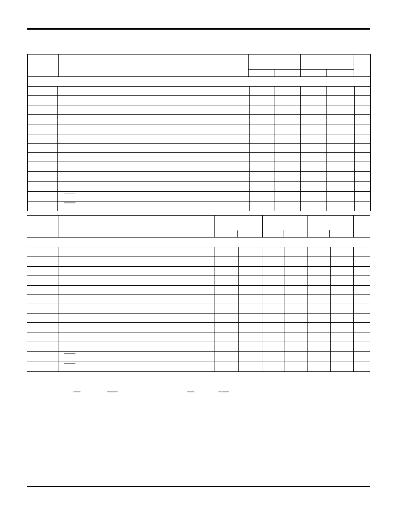
IDT7016S/L
HIGH-SPEED 16K x 9 DUAL-PORT STATIC RAM
MILITARY AND COMMERCIAL TEMPERATURE RANGES
6.13
9
IDT7016X20
IDT7016X25
IDT7016X35
Symbol
WRITE CYCLE
t
WC
t
EW
t
AW
t
AS
t
WP
t
WR
t
DW
t
HZ
Parameter
Min.
Max.
Min.
Max.
Min.
Max.
Unit
Write Cycle Time
Chip Enable to End-of-Write
(3)
Address Valid to End-of-Write
Address Set-up Time
(3)
Write Pulse Width
Write Recovery Time
Data Valid to End-of-Write
Output High-Z Time
(1, 2)
Data Hold Time
(4)
Write Enable to Output in High-Z
(1, 2)
Output Active from End-of-Write
(1, 2, 4)
20
15
15
0
15
2
15
—
—
—
—
—
—
—
—
12
25
20
20
0
20
2
15
—
—
—
—
—
—
—
—
15
35
30
30
0
25
2
15
—
—
—
—
—
—
—
—
20
ns
ns
ns
ns
ns
ns
ns
ns
t
DH
0
—
0
—
0
—
ns
t
WZ
t
OW
—
3
12
—
—
3
15
—
—
3
20
—
ns
ns
t
SWRD
SEM
Flag Write to Read Time
5
—
5
—
5
—
ns
t
SPS
SEM
Flag Contention Window
5
—
5
—
5
—
ns
AC ELECTRICAL CHARACTERISTICS OVER THE
OPERATING TEMPERATURE AND SUPPLY VOLTAGE
(5)
IDT7016X12
Com'l. Only
Min.
IDT7016X15
Com'l. Only
Min.
Symbol
WRITE CYCLE
t
WC
t
EW
t
AW
t
AS
t
WP
t
WR
t
DW
Parameter
Max
Max.
Unit
Write Cycle Time
Chip Enable to End-of-Write
(3)
Address Valid to End-of-Write
Address Set-up Time
(3)
Write Pulse Width
Write Recovery Time
Data Valid to End-of-Write
Output High-Z Time
(1, 2)
Data Hold Time
(4)
Write Enable to Output in High-Z
(1, 2)
Output Active from End-of-Write
(1, 2, 4)
12
10
10
0
10
2
10
—
—
—
—
—
—
—
15
12
12
0
12
2
10
—
—
—
—
—
—
—
ns
ns
ns
ns
ns
ns
ns
t
HZ
—
10
—
10
ns
t
DH
t
WZ
0
—
—
10
0
—
—
10
ns
ns
t
OW
3
—
3
—
ns
t
SWRD
t
SPS
SEM
Flag Write to Read Time
SEM
Flag Contention Window
5
5
—
—
5
5
—
—
ns
ns
NOTES:
1. Transition is measured
±
200mV from Low or High-impedance voltage with the Output Test Load (Figure 2).
2. This parameter is guaranteed by device characterization but not production tested.
3. To access RAM,
CE
= V
IL
and
SEM
= V
IH
. To access semaphore,
CE
= V
IH
and
SEM
= V
IL
. Either condition must be valid for the entire t
EW
time.
4. The specification for t
DH
must be met by the device supplying write data to the RAM under all operating conditions. Although t
DH
and t
OW
values will vary
over voltage and temperature, the actual t
DH
will always be smaller than the actual t
OW
.
5. "X" in part numbers indicates power rating (S or L).
3190 tbl 12
相關(guān)PDF資料 |
PDF描述 |
|---|---|
| IDT7016S12GB | Low-Power JFET-Input Quad Operational Amplifier 14-CFP -55 to 125 |
| IDT7016S12J | Low-Power JFET-Input Quad Operational Amplifier 20-LCCC -55 to 125 |
| IDT7016S12JB | Low-Power JFET-Input Quad Operational Amplifier 20-LCCC -55 to 125 |
| IDT7016S12PF | Low-Power JFET-Input Quad Operational Amplifier 14-CDIP -55 to 125 |
| IDT7016S12PFB | Low-Power JFET-Input Quad Operational Amplifier 14-CDIP -55 to 125 |
相關(guān)代理商/技術(shù)參數(shù) |
參數(shù)描述 |
|---|---|
| IDT7016S12GB | 制造商:IDT 制造商全稱:Integrated Device Technology 功能描述:HIGH-SPEED 16K x 9 DUAL-PORT STATIC RAM |
| IDT7016S12GG | 制造商:IDT 制造商全稱:Integrated Device Technology 功能描述:HIGH-SPEED 16K X 9 DUAL-PORT STATIC RAM |
| IDT7016S12GGB | 制造商:IDT 制造商全稱:Integrated Device Technology 功能描述:HIGH-SPEED 16K X 9 DUAL-PORT STATIC RAM |
| IDT7016S12GGI | 制造商:IDT 制造商全稱:Integrated Device Technology 功能描述:HIGH-SPEED 16K X 9 DUAL-PORT STATIC RAM |
| IDT7016S12J | 功能描述:IC SRAM 144KBIT 12NS 68PLCC RoHS:否 類別:集成電路 (IC) >> 存儲(chǔ)器 系列:- 標(biāo)準(zhǔn)包裝:1,000 系列:- 格式 - 存儲(chǔ)器:RAM 存儲(chǔ)器類型:SRAM - 雙端口,同步 存儲(chǔ)容量:1.125M(32K x 36) 速度:5ns 接口:并聯(lián) 電源電壓:3.15 V ~ 3.45 V 工作溫度:-40°C ~ 85°C 封裝/外殼:256-LBGA 供應(yīng)商設(shè)備封裝:256-CABGA(17x17) 包裝:帶卷 (TR) 其它名稱:70V3579S5BCI8 |
發(fā)布緊急采購(gòu),3分鐘左右您將得到回復(fù)。