- 您現(xiàn)在的位置:買(mǎi)賣(mài)IC網(wǎng) > PDF目錄377352 > IDT71V67902S80BGI (INTEGRATED DEVICE TECHNOLOGY INC) 256K X 36, 512K X 18 3.3V Synchronous SRAMs 2.5V I/O, Burst Counter Flow-Through Outputs, Single Cycle Deselect PDF資料下載
參數(shù)資料
| 型號(hào): | IDT71V67902S80BGI |
| 廠商: | INTEGRATED DEVICE TECHNOLOGY INC |
| 元件分類(lèi): | DRAM |
| 英文描述: | 256K X 36, 512K X 18 3.3V Synchronous SRAMs 2.5V I/O, Burst Counter Flow-Through Outputs, Single Cycle Deselect |
| 中文描述: | 512K X 18 CACHE SRAM, 8 ns, PBGA119 |
| 封裝: | 14 X 22 MM, PLASTIC, BGA-119 |
| 文件頁(yè)數(shù): | 2/23頁(yè) |
| 文件大?。?/td> | 527K |
| 代理商: | IDT71V67902S80BGI |
第1頁(yè)當(dāng)前第2頁(yè)第3頁(yè)第4頁(yè)第5頁(yè)第6頁(yè)第7頁(yè)第8頁(yè)第9頁(yè)第10頁(yè)第11頁(yè)第12頁(yè)第13頁(yè)第14頁(yè)第15頁(yè)第16頁(yè)第17頁(yè)第18頁(yè)第19頁(yè)第20頁(yè)第21頁(yè)第22頁(yè)第23頁(yè)
6.42
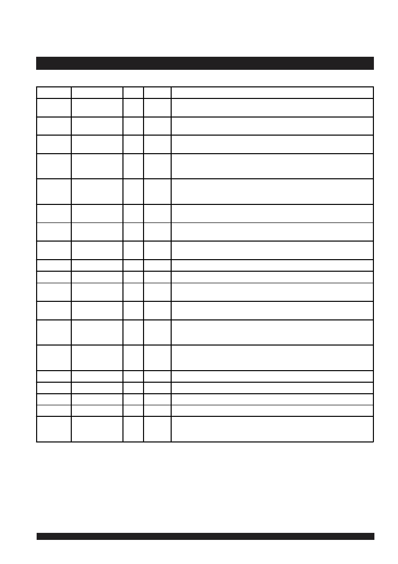
IDT71V67702, IDT71V67902, 256K x 36, 512K x 18, 3.3V Synchronous Commercial and Industrial Temperature Ranges
SRAMs with 2.5V I/O, Flow-Through Outputs, Single Cycle Deselect
Symbol
Pin Function
I/O
Active
Description
A
0
-A
18
Address Inputs
I
N/A
Synchronous Address inputs. The address register is triggered by a combi-nation of the
rising edge of CLK and
ADSC
Lowor
ADSP
Lowand
CE
Low
ADSC
Address Status
(Cache Controller)
I
LOW
Synchronous Address Status fromCache Controller
ADSC
is an active LOW input that is
used to load the address registers wth newaddresses.
ADSP
Address Status
(Processor)
I
LOW
Synchronous Address Status fromProcessor
ADSP
is an active LOW input that is used to
load the address registers wth newaddresses.
ADSP
is gated by
CE
.
ADV
Burst Address
Advance
I
LOW
Synchronous Address Advance.
ADV
is an active LOW input that is used to advance the
internal burst counter controlling burst access after the initial address is loaded. When the
input is HIGH the burst counter is not incremented; that is, there is no address advance.
BWE
Byte Write Enable
I
LOW
Synchronous byte write enable gates the byte write inputs
BW
1
-
BW
4
. If
BWE
is LOW at the
rising edge of CLK then
BW
x inputs are passed to the next stage in the circuit. If
BWE
is
HIGH then the byte write inputs are blocked and only
GW
can initiate a write cycle.
BW
1
-
BW
4
Individual Byte
Write Enables
I
LOW
Synchronous byte write enables.
BW
1
controls I/O
0-7
, I/O
P1
,
BW
2
controls I/O
8-15
, I/O
P2
, etc.
Any active byte write causes all outputs to be disabled.
CE
Chip Enable
I
LOW
Synchronous chip enable.
CE
is used wth CS
0
and
CS
1
to enable the IDT71V67702/7902.
CE
also gates
ADSP
.
CLK
Clock
I
N/A
This is the clock input. All timng references for the device are made wth respect to this
input.
CS
0
Chip Select 0
I
HIGH
Synchronous active HIGH chip select. CS
0
is used wth
CE
and
CS
1
to enable the chip.
CS
1
Chip Select 1
I
LOW
Synchronous active LOW chip select.
CS
1
is used wth
CE
and CS
0
to enable the chip.
GW
Global Write
Enable
I
LOW
Synchronous global write enable. This input wll write all four 9-bit data bytes when LOW
on the rising edge of CLK.
GW
supersedes individual byte write enables.
I/O
0
-I/O
31
I/O
P1
-I/O
P4
Data Input/Output
I/O
N/A
Synchronous data input/output (I/O) pins. The data input path is registered, triggered by
the rising edge of CLK. The data output path is flow-through (no output register).
LBO
Linear Burst Order
I
LOW
Asynchronous burst order selection input. When
LBO
is HIGH, the inter-leaved burst
sequence is selected. When
LBO
is LOW the Linear burst sequence is selected.
LBO
is a
static input and must not change state while the device is operating.
OE
Output Enable
I
LOW
Asynchronous output enable. When
OE
is LOW the data output drivers are enabled on the
I/O pins if the chip is also selected. When
OE
is HIGH the I/O pins are in a high-
impedance state.
V
DD
Power Supply
N/A
N/A
3.3V core power supply.
V
DDQ
Power Supply
N/A
N/A
2.5V I/O Supply.
V
SS
Ground
N/A
N/A
Ground.
NC
No Connect
N/A
N/A
NC pins are not electrically connected to the device.
ZZ
Sleep Mode
1
HIGH
Asynchronous sleep mode input. ZZ HIGH wll gate the CLK internally and power down
the IDT71V67702/7902 to its lowest power consumption level. Data retention is guaranteed
in Sleep Mode.
5317t tbl 02
Pin Definitions
(1)
NOTE:
1. All synchronous inputs must meet specified setup and hold times with respect to CLK.
相關(guān)PDF資料 |
PDF描述 |
|---|---|
| IDT71V67902S80BQ | 256K X 36, 512K X 18 3.3V Synchronous SRAMs 2.5V I/O, Burst Counter Flow-Through Outputs, Single Cycle Deselect |
| IDT71V67902S80BQI | 256K X 36, 512K X 18 3.3V Synchronous SRAMs 2.5V I/O, Burst Counter Flow-Through Outputs, Single Cycle Deselect |
| IDT71V67902S80PF | 256K X 36, 512K X 18 3.3V Synchronous SRAMs 2.5V I/O, Burst Counter Flow-Through Outputs, Single Cycle Deselect |
| IDT71V67902S80PFI | 256K X 36, 512K X 18 3.3V Synchronous SRAMs 2.5V I/O, Burst Counter Flow-Through Outputs, Single Cycle Deselect |
| IDT71V67902S85BG | 256K X 36, 512K X 18 3.3V Synchronous SRAMs 2.5V I/O, Burst Counter Flow-Through Outputs, Single Cycle Deselect |
相關(guān)代理商/技術(shù)參數(shù) |
參數(shù)描述 |
|---|---|
| IDT71V67903S75BG | 功能描述:IC SRAM 9MBIT 75NS 119BGA RoHS:否 類(lèi)別:集成電路 (IC) >> 存儲(chǔ)器 系列:- 標(biāo)準(zhǔn)包裝:72 系列:- 格式 - 存儲(chǔ)器:RAM 存儲(chǔ)器類(lèi)型:SRAM - 同步 存儲(chǔ)容量:9M(256K x 36) 速度:75ns 接口:并聯(lián) 電源電壓:3.135 V ~ 3.465 V 工作溫度:-40°C ~ 85°C 封裝/外殼:100-LQFP 供應(yīng)商設(shè)備封裝:100-TQFP(14x14) 包裝:托盤(pán) 其它名稱(chēng):71V67703S75PFGI |
| IDT71V67903S75BG8 | 功能描述:IC SRAM 9MBIT 75NS 119BGA RoHS:否 類(lèi)別:集成電路 (IC) >> 存儲(chǔ)器 系列:- 標(biāo)準(zhǔn)包裝:72 系列:- 格式 - 存儲(chǔ)器:RAM 存儲(chǔ)器類(lèi)型:SRAM - 同步 存儲(chǔ)容量:9M(256K x 36) 速度:75ns 接口:并聯(lián) 電源電壓:3.135 V ~ 3.465 V 工作溫度:-40°C ~ 85°C 封裝/外殼:100-LQFP 供應(yīng)商設(shè)備封裝:100-TQFP(14x14) 包裝:托盤(pán) 其它名稱(chēng):71V67703S75PFGI |
| IDT71V67903S75BQ | 功能描述:IC SRAM 9MBIT 75NS 165FBGA RoHS:否 類(lèi)別:集成電路 (IC) >> 存儲(chǔ)器 系列:- 標(biāo)準(zhǔn)包裝:72 系列:- 格式 - 存儲(chǔ)器:RAM 存儲(chǔ)器類(lèi)型:SRAM - 同步 存儲(chǔ)容量:9M(256K x 36) 速度:75ns 接口:并聯(lián) 電源電壓:3.135 V ~ 3.465 V 工作溫度:-40°C ~ 85°C 封裝/外殼:100-LQFP 供應(yīng)商設(shè)備封裝:100-TQFP(14x14) 包裝:托盤(pán) 其它名稱(chēng):71V67703S75PFGI |
| IDT71V67903S75BQ8 | 功能描述:IC SRAM 9MBIT 75NS 165FBGA RoHS:否 類(lèi)別:集成電路 (IC) >> 存儲(chǔ)器 系列:- 標(biāo)準(zhǔn)包裝:72 系列:- 格式 - 存儲(chǔ)器:RAM 存儲(chǔ)器類(lèi)型:SRAM - 同步 存儲(chǔ)容量:9M(256K x 36) 速度:75ns 接口:并聯(lián) 電源電壓:3.135 V ~ 3.465 V 工作溫度:-40°C ~ 85°C 封裝/外殼:100-LQFP 供應(yīng)商設(shè)備封裝:100-TQFP(14x14) 包裝:托盤(pán) 其它名稱(chēng):71V67703S75PFGI |
| IDT71V67903S75BQG | 功能描述:IC SRAM 9MBIT 75NS 165FBGA RoHS:是 類(lèi)別:集成電路 (IC) >> 存儲(chǔ)器 系列:- 標(biāo)準(zhǔn)包裝:72 系列:- 格式 - 存儲(chǔ)器:RAM 存儲(chǔ)器類(lèi)型:SRAM - 同步 存儲(chǔ)容量:9M(256K x 36) 速度:75ns 接口:并聯(lián) 電源電壓:3.135 V ~ 3.465 V 工作溫度:-40°C ~ 85°C 封裝/外殼:100-LQFP 供應(yīng)商設(shè)備封裝:100-TQFP(14x14) 包裝:托盤(pán) 其它名稱(chēng):71V67703S75PFGI |
發(fā)布緊急采購(gòu),3分鐘左右您將得到回復(fù)。