- 您現(xiàn)在的位置:買賣IC網(wǎng) > PDF目錄377397 > IDT7210L35GB (Integrated Device Technology, Inc.) High-Performance Current-Mode PWM Controller 8-PDIP -40 to 85 PDF資料下載
參數(shù)資料
| 型號: | IDT7210L35GB |
| 廠商: | Integrated Device Technology, Inc. |
| 英文描述: | High-Performance Current-Mode PWM Controller 8-PDIP -40 to 85 |
| 中文描述: | 16 × 16并行CMOS乘法累加器 |
| 文件頁數(shù): | 1/10頁 |
| 文件大小: | 167K |
| 代理商: | IDT7210L35GB |
Integrated Device Technology, Inc.
MILITARY AND COMMERCIAL TEMPERATURE RANGES
AUGUST 1995
1995 Integrated Device Technology, Inc.
11.2
DSC-2018/7
1
IDT7210L
16 x 16 PARALLEL CMOS
MULTIPLIER-ACCUMULATOR
FEATURES:
16 x 16 parallel multiplier-accumulator with selectable
accumulation and subtraction
High-speed: 20ns multiply-accumulate time
IDT7210 features selectable accumulation, subtraction,
rounding and preloading with 35-bit result
IDT7210 is pin and function compatible with the TRW
TDC1010J, TMC2210, Cypress CY7C510, and AMD
AM29510
Performs subtraction and double precision addition and
multiplication
Produced using advanced CMOS high-performance
technology
TTL-compatible
Available in topbraze DIP, PLCC, Flatpack and Pin Grid
Array
Military product compliant to MIL-STD-883, Class B
Standard Military Drawing #5962-88733 is listed on this
function
Speeds available:
Commercial: L20/25/35/45/55/65
Military:
L25/30/40/55/65/75
DESCRIPTION:
The IDT7210 is a high-speed, low-power 16 x 16-bit parallel
multiplier-accumulator that is ideally suited for real-time digital
signal processing applications. Fabricated using CMOS
silicon gate technology, this device offers a very low-power
alternative to existing bipolar and NMOS counterparts, with
only 1/7 to 1/10 the power dissipation and exceptional speed
(25ns maximum) performance.
A pin and functional replacement for TRW’s TDC1010J the
IDT7210 operates from a single 5 volt supply and is compatible
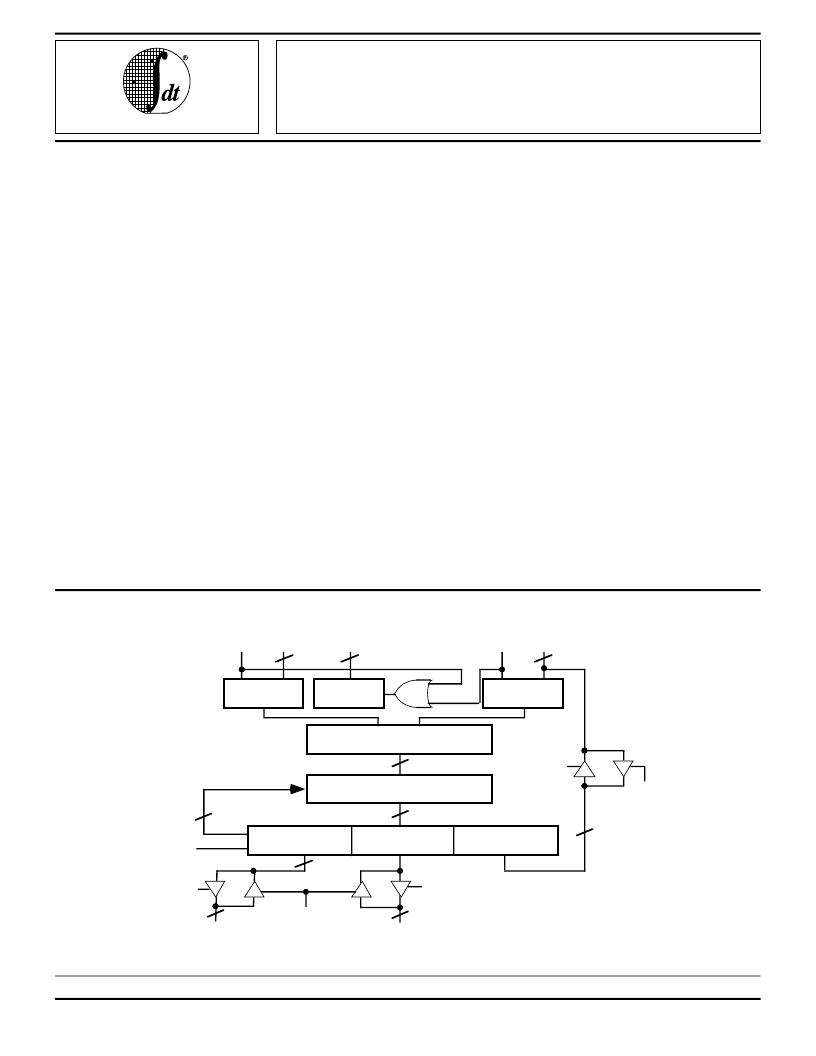
with standard TTL logic levels. The architecture of the IDT7210
is fairly straightforward, featuring individual input and output
registers with clocked D-type flip-flop, a preload capability
which enables input data to be preloaded into the output
registers, individual three-state output ports for the Extended
Product (XTP) and Most Significant Product (MSP) and a
Least Significant Product output (LSP) which is multiplexed
with the Y input.
The X
IN
and Y
IN
data input registers may be specified
through the use of the Two’s Complement input (TC) as either
a two’s complement or an unsigned magnitude, yielding a full-
precision 32-bit result that may be accumulated to a full 35-bit
result. The three output registers – Extended Product (XTP),
Most Most Significant Product (MSP) and Least Significant
Product (LSP) – are controlled by the respective TSX, TSM
and TSL input lines. The LSP output can be routed through Y
IN
ports.
FUNCTIONAL BLOCK DIAGRAM
MULTIPLIER ARRAY
ACCUMULATOR
MSP REGISTER
LSP REGISTER
XTP REGISTER
16
TSL
16
XTP
OUT
(P
34
-P
32
)
3
3
35
+/–
TSX
PREL
CLKP
35
32
YREGISTER
REGISTER
XREGISTER
CONTROL
16
4
16
CLKX
CLKY
RND, TC
ACC, SUB,
X
IN
(X
15
-X
0
)
Y
IN
(Y
15
-Y
0
/P
15
-P
0
)
TSM
MSP
OUT
(P
31
-P
16
)
IDT7210
2577 drw 01
PREL
+
相關PDF資料 |
PDF描述 |
|---|---|
| IDT7210L35J | High-Performance Current-Mode PWM Controller 8-PDIP -40 to 85 |
| IDT7210L35JB | JFET-input Operational Amplifiers 8-PDIP 0 to 70 |
| IDT7210L40C | JFET-input Operational Amplifiers 8-PDIP 0 to 70 |
| IDT7210L40CB | 16 x 16 PARALLEL CMOS MULTIPLIER-ACCUMULATOR |
| IDT7210L40F | 16 x 16 PARALLEL CMOS MULTIPLIER-ACCUMULATOR |
相關代理商/技術參數(shù) |
參數(shù)描述 |
|---|---|
| IDT7210L35J | 制造商:Integrated Device Technology Inc 功能描述: |
| IDT7210L40FB | 制造商:Integrated Device Technology Inc 功能描述: |
| IDT7210L45J | 制造商:Integrated Device Technology Inc 功能描述: |
| IDT7210L65P | 制造商:Integrated Device Technology Inc 功能描述: 制造商:Integrated Device Technology Inc 功能描述:MULTIPLIER/ACCUMULATOR, 64 Pin, Plastic, DIP |
| IDT72125L25SO | 功能描述:IC FIFO 1KX16 PAR-SER 28SOIC RoHS:否 類別:集成電路 (IC) >> 邏輯 - FIFO 系列:7200 標準包裝:90 系列:7200 功能:同步 存儲容量:288K(16K x 18) 數(shù)據(jù)速率:100MHz 訪問時間:10ns 電源電壓:4.5 V ~ 5.5 V 工作溫度:0°C ~ 70°C 安裝類型:表面貼裝 封裝/外殼:64-LQFP 供應商設備封裝:64-TQFP(14x14) 包裝:托盤 其它名稱:72271LA10PF |
發(fā)布緊急采購,3分鐘左右您將得到回復。