- 您現(xiàn)在的位置:買賣IC網(wǎng) > PDF目錄377397 > IDT7210L35JB (Integrated Device Technology, Inc.) JFET-input Operational Amplifiers 8-PDIP 0 to 70 PDF資料下載
參數(shù)資料
| 型號: | IDT7210L35JB |
| 廠商: | Integrated Device Technology, Inc. |
| 英文描述: | JFET-input Operational Amplifiers 8-PDIP 0 to 70 |
| 中文描述: | 16 × 16并行CMOS乘法累加器 |
| 文件頁數(shù): | 5/10頁 |
| 文件大?。?/td> | 167K |
| 代理商: | IDT7210L35JB |
11.2
5
IDT7210L
16 x 16 PARALLEL CMOS MULTIPLIER-ACCUMULATOR
MILITARY AND COMMERCIAL TEMPERATURE RANGES
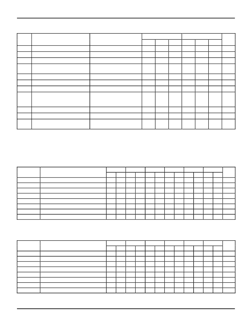
DC ELECTRICAL CHARACTERISTICS
(Commercial: V
CC
= 5.0V
±
10%, T
A
= 0
°
C to +70
°
C; Military: V
CC
= 5V
±
10%, T
A
= –55
°
C to +125
°
C)
AC ELECTRICAL CHARACTERISTICS MILITARY
(V
CC
= 5V
±
10%, T
A
= –55
°
to +125
°
C)
NOTES:
1. Transition is measured
±
500mV from steady state voltage.
2. Minimum delays guaranteed but not tested
2577 tbl 07
NOTES:
1. Typical implies V
CC
= 5V and T
A
= +25
°
C.
2. I
CC
is measured at 10MHz and V
IN
= 0 to 3V. For frequencies greater than 10MHz, the following equation is used for the commercial range:
I
CC
= 90+ 6(f –10)mA, where f = operating frequency in MHz. For the military range, I
CC
= 110 + 8(f –10). f = operating frequency in MHz, f = 1/t
MA
.
3. For frequencies greater than 10MHz, guaranteed by design, not production tested.
4. I
OL
= 4mA for t
MA
> 55ns.
5. For conditions shown as Max. or Min., use appropriate value specified under electrical characteristics.
2577 tbl 05
AC ELECTRICAL CHARACTERISTICS COMMERCIAL
(V
CC
= 5V
±
10%, T
A
= 0
°
to +70
°
C)
7210L20
Symbol
Parameter
Min. Max. Min. Max. Min. Max. Min. Max. Min. Max. Min. Max. Unit
t
MA
Multiply-Accumulate Time
(2)
2.0
20
t
D
Output Delay
(2)
2.0
18
t
ENA
3-State Enable Time
—
18
t
DIS
3-State Disable Time
(1)
—
18
t
S
Input Register Set-up Time
10
—
t
H
Input Register Hold Time
3
—
t
PW
Clock Pulse Width
9
—
t
HCL
Relative Hold Time
0
—
NOTES:
1. Transition is measured
±
500mV from steady state voltage.
2. Minimum delays guaranteed but not tested
2577 tbl 06
Commercial
Min.
Typ.
(1)
2.0
—
Military
Typ.
(1)
—
—
Symbol
V
IH
V
IL
Parameter
Test Conditions
(5)
Guaranteed Logic HIGH Level
Guaranteed Logic LOW Level
Max.
—
0.8
Min.
2.0
—
Max.
—
0.8
Unit
V
V
μ
A
μ
A
Input High Voltage
Input Low Voltage
—
—
|I
LI
|
|I
LO
|
Input Leakage Current
Output Leakage Current
V
CC
= Max., V
IN
= 0V to
V
CC
V
CC
= Max., Outputs Disabled
V
OUT
= 0 to
V
CC
V
CC
= Min., I
OH
= –2.0mA
—
—
—
—
10
10
—
—
—
—
10
10
V
OH
V
OL(4)
I
OS
I
CC(2)
Output HIGH Voltage
2.4
—
—
2.4
—
—
V
Output LOW Voltage
Output Short Circuit Current
Operating Power Supply Current
V
CC
= Min., I
OL
= 4mA
V
CC
= Max., V
0
GND
V
CC
= Max., Outputs Enabled
f= 10MHz
(2)
C
L
= 50 pF
V
IN
≥
V
IH
, V
IN
≤
V
IL
V
IN
≥
V
CC
–0.2V, V
IN
≤
0.2V
V
CC
= Max., Outputs Disabled
—
-20
—
—
—
45
0.4
-100
90
—
-20
—
—
—
45
0.4
-100
110
V
mA
mA
I
CCQ1
I
CCQ2
I
CC
/f
(2,3)
Increase in Power Supply
Current MHz
Quiescent Power Supply Current
Quiescent Power Supply Current
—
—
—
20
4
—
30
10
6
—
—
—
20
4
—
30
12
8
mA
mA
mA/
MHz
7210L25
Min. Max. Min. Max. Min. Max. Min. Max. Min. Max. Min. Max. Unit
2.0
25
2.0
30
2.0
40
2.0
2.0
20
2.0
20
2.0
25
2.0
—
20
–
20
–
25
–
—
20
–
20
–
25
–
12
—
12
–
15
–
20
3
—
3
–
3
–
3
10
—
10
–
15
–
20
0
—
0
–
0
–
0
7210L30
7210L40
7210L55
7210L65
7210L75
Symbol
t
MA
t
D
t
ENA
t
DIS
t
S
t
H
t
PW
t
HCL
Parameter
Multiply-Accumulate Time
(2)
Output Delay
(2)
3-State Enable Time
3-State Disable Time
(1)
Input Register Set-up Time
Input Register Hold Time
Clock Pulse Width
Relative Hold Time
55
30
30
25
–
–
–
–
2.0
2.0
–
–
25
3
25
0
65
35
30
30
–
–
–
–
2.0
2.0
–
–
25
3
25
0
75
35
35
30
–
–
–
–
ns
ns
ns
ns
ns
ns
ns
ns
7210L25
7210L35
7210L45
7210L55
7210L65
2.0
2.0
–
–
12
3
10
0
25
20
20
20
–
–
–
–
2.0
2.0
–
–
12
3
10
0
35
25
25
25
–
–
–
–
2.0
2.0
–
–
15
3
15
0
45
25
25
25
–
–
–
–
2.0
2.0
–
–
20
3
20
0
55
30
30
30
–
–
–
–
2.0
2.0
–
–
25
3
25
0
65
35
30
30
–
–
–
–
ns
ns
ns
ns
ns
ns
ns
ns
相關PDF資料 |
PDF描述 |
|---|---|
| IDT7210L40C | JFET-input Operational Amplifiers 8-PDIP 0 to 70 |
| IDT7210L40CB | 16 x 16 PARALLEL CMOS MULTIPLIER-ACCUMULATOR |
| IDT7210L40F | 16 x 16 PARALLEL CMOS MULTIPLIER-ACCUMULATOR |
| IDT7210L40FB | 16 x 16 PARALLEL CMOS MULTIPLIER-ACCUMULATOR |
| IDT7210L40G | 16 x 16 PARALLEL CMOS MULTIPLIER-ACCUMULATOR |
相關代理商/技術參數(shù) |
參數(shù)描述 |
|---|---|
| IDT7210L40FB | 制造商:Integrated Device Technology Inc 功能描述: |
| IDT7210L45J | 制造商:Integrated Device Technology Inc 功能描述: |
| IDT7210L65P | 制造商:Integrated Device Technology Inc 功能描述: 制造商:Integrated Device Technology Inc 功能描述:MULTIPLIER/ACCUMULATOR, 64 Pin, Plastic, DIP |
| IDT72125L25SO | 功能描述:IC FIFO 1KX16 PAR-SER 28SOIC RoHS:否 類別:集成電路 (IC) >> 邏輯 - FIFO 系列:7200 標準包裝:90 系列:7200 功能:同步 存儲容量:288K(16K x 18) 數(shù)據(jù)速率:100MHz 訪問時間:10ns 電源電壓:4.5 V ~ 5.5 V 工作溫度:0°C ~ 70°C 安裝類型:表面貼裝 封裝/外殼:64-LQFP 供應商設備封裝:64-TQFP(14x14) 包裝:托盤 其它名稱:72271LA10PF |
| IDT72125L25SO8 | 功能描述:IC FIFO 1KX16 PAR-SER 28SOIC RoHS:否 類別:集成電路 (IC) >> 邏輯 - FIFO 系列:7200 標準包裝:90 系列:7200 功能:同步 存儲容量:288K(16K x 18) 數(shù)據(jù)速率:100MHz 訪問時間:10ns 電源電壓:4.5 V ~ 5.5 V 工作溫度:0°C ~ 70°C 安裝類型:表面貼裝 封裝/外殼:64-LQFP 供應商設備封裝:64-TQFP(14x14) 包裝:托盤 其它名稱:72271LA10PF |
發(fā)布緊急采購,3分鐘左右您將得到回復。