- 您現(xiàn)在的位置:買賣IC網(wǎng) > PDF目錄377405 > IDT72225LB15G (INTEGRATED DEVICE TECHNOLOGY INC) CMOS SyncFIFOO 256 x 18, 512 x 18, 1024 x 18, 2048 x 18 and 4096 x 18 PDF資料下載
參數(shù)資料
| 型號: | IDT72225LB15G |
| 廠商: | INTEGRATED DEVICE TECHNOLOGY INC |
| 元件分類: | DRAM |
| 英文描述: | CMOS SyncFIFOO 256 x 18, 512 x 18, 1024 x 18, 2048 x 18 and 4096 x 18 |
| 中文描述: | 1K X 18 OTHER FIFO, CPGA68 |
| 封裝: | CAVITY-UP, PGA-68 |
| 文件頁數(shù): | 6/16頁 |
| 文件大小: | 181K |
| 代理商: | IDT72225LB15G |
6
IDT72205LB/72215LB/72225LB/72235LB/72245LB CMOS SyncFIFO
256 x 18, 512 x 18, 1,024 x 18, 2,048 x 18 and 4,096 x 18
Commercial And Industrial Temperature Ranges
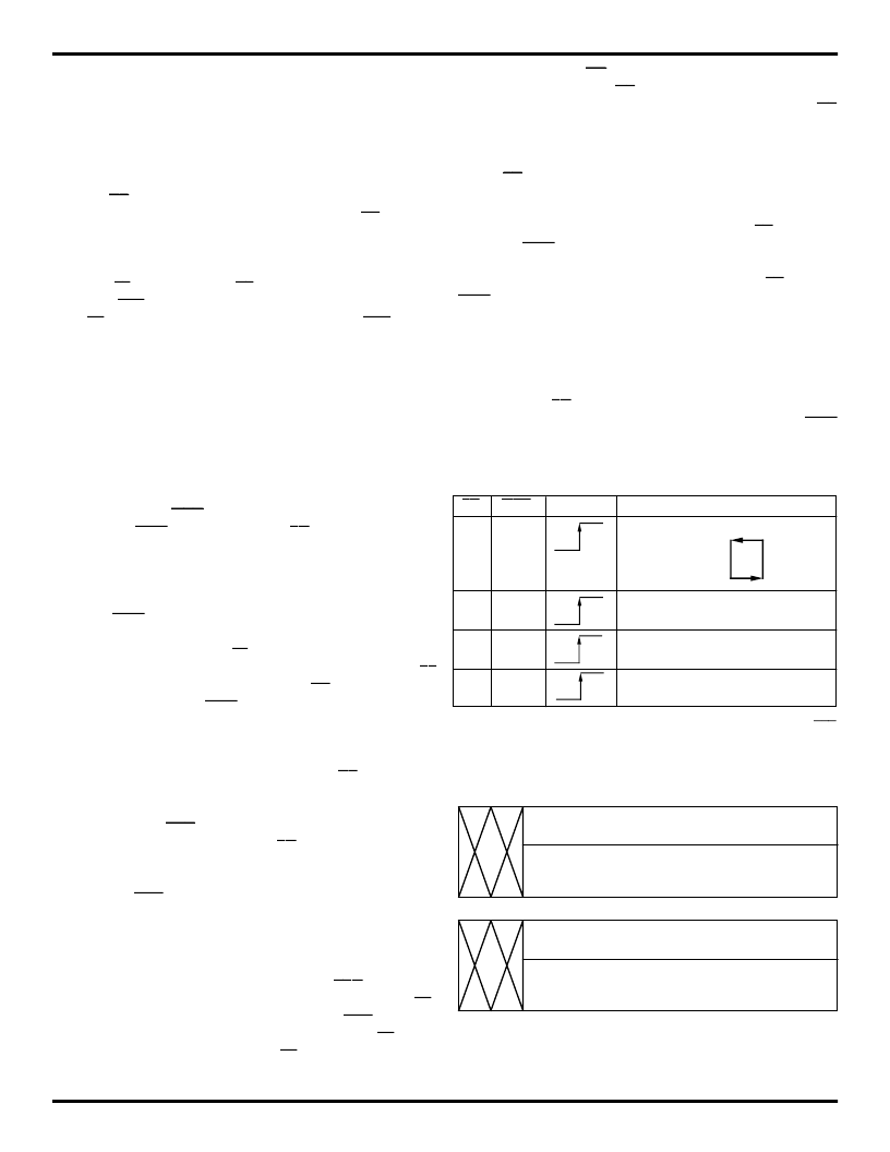
LD
WEN
WCLK
Selection
0
0
Writing to offset registers:
Empty Offset
Full Offset
0
1
No Operation
1
0
Write Into FIFO
1
1
No Operation
NOTE:
1. The same selection sequence applies to reading from the registers.
REN
is enabled and read is performed on the LOW-to-HIGH transition of
RCLK.
Figure 2. Write Offset Register
2766 tbl 08
NOTE:
1. Any bits of the offset register not being programmed should be set to zero.
Figure 3. Offset Register Location and Default Values
EMPTY OFFSET REGISTER
17
11
0
001FH (72205) 003FH (72215):
007FH (72225/72235/72245)
FULL OFFSET REGISTER
17
11
0
DEFAULT VALUE
DEFAULT VALUE
001FH (72205) 003FH (72215):
007FH (72225/72235/72245)
2766 drw 05
SIGNAL DESCRIPTIONS:
INPUTS:
DATA IN (D
0
- D
17
)
Data inputs for 18-bit wide data.
CONTROLS:
RESET (
RS
)
Reset is accomplished whenever the Reset (
RS
) input is
taken to a LOW state. During reset, both internal read and
write pointers are set to the first location. A reset is required
after power-up before a write operation can take place. The
Full Flag (
FF
), Half-Full Flag (
HF
) and Programmable Almost-
Full Flag (
PAF
) will be reset to HIGH after t
RSF
. The Empty
Flag (
EF
) and Programmable Almost-Empty Flag (
PAE
) will be
reset to LOW after t
RSF
. During reset, the output register is
initialized to all zeros and the offset registers are initialized to
their default values.
WRITE CLOCK (WCLK)
A write cycle is initiated on the LOW-to-HIGH transition of the
write clock (WCLK). Data set-up and hold times must be met with
respect to the LOW-to-HIGH transition of the write clock (WCLK).
The write and read clocks can be asynchronous or coincident.
WRITE ENABLE (
When the
WEN
input is LOW and
LD
input is HIGH, data
may be loaded into the FIFO RAM array on the rising edge of
every WCLK cycle if the device is not full. Data is stored in the
RAM array sequentially and independently of any ongoing
read operation.
When
WEN
is HIGH, no new data is written in the RAM
array on each WCLK cycle.
To prevent data overflow,
FF
will go LOW, inhibiting further
write operations. Upon the completion of a valid read cycle,
FF
will go HIGH allowing a write to occur. The
FF
flag is updated on
the rising edge of WCLK.
WEN
is ignored when the FIFO is full.
WEN
)
READ CLOCK (RCLK)
Data can be read on the outputs on the LOW-to-HIGH transition
of the read clock (RCLK), when Output Enable (
OE
) is set LOW.
The write and read clocks can be asynchronous or coincident.
READ ENABLE (
When Read Enable is LOW and
LD
input is HIGH, data is
loaded from the RAM array into the output register on the
rising edge of every RCLK cycle if the device is not empty.
When the
REN
input is HIGH, the output register holds the
previous data and no new data is loaded into the output
register. The data outputs Q
0
-Q
n
maintain the previous data
value.
Every word accessed at Q
n
, including the first word written
to an empty FIFO, must be requested using
REN
. When the
last word has been read from the FIFO, the Empty Flag (
EF
)
will go LOW, inhibiting further read operations.
REN
is ignored
when the FIFO is empty. Once a write is performed,
EF
will go
HIGH allowing a read to occur. The
EF
flag is updated on the
rising edge of RCLK.
REN
)
OUTPUT ENABLE (
When Output Enable (
OE
) is enabled (LOW), the parallel
output buffers receive data from the output register. When
OE
is disabled (HIGH), the Q output data bus is in a high-
impedance state.
OE
)
LOAD (
The IDT72205LB/72215LB/72225LB/72235LB/72245LB
devices contain two 12-bit offset registers with data on the
inputs, or read on the outputs. When the Load (
LD
) pin is set
LOW and
WEN
is set LOW, data on the inputs D0-D11 is
written into the Empty offset register on the first LOW-to-HIGH
transition of the write clock (WCLK). When the
LD
pin and
(
WEN
) are held LOW then data is written into the Full offset
register on the second LOW-to-HIGH transition of the write
clock (WCLK). The third transition of the write clock (WCLK)
again writes to the Empty offset register.
However, writing all offset registers does not have to occur
at one time. One or two offset registers can be written and then
by bringing the
LD
pin HIGH, the FIFO is returned to normal
read/write operation. When the LD pin is set LOW, and
WEN
is LOW, the next offset register in sequence is written.
LD
)
相關(guān)PDF資料 |
PDF描述 |
|---|---|
| IDT72225LB15GB | CMOS SyncFIFOO 256 x 18, 512 x 18, 1024 x 18, 2048 x 18 and 4096 x 18 |
| IDT72225LB15J | CMOS SyncFIFOO 256 x 18, 512 x 18, 1024 x 18, 2048 x 18 and 4096 x 18 |
| IDT72225LB15JB | CMOS SyncFIFOO 256 x 18, 512 x 18, 1024 x 18, 2048 x 18 and 4096 x 18 |
| IDT72225LB15JI | CMOS SyncFIFOO 256 x 18, 512 x 18, 1024 x 18, 2048 x 18 and 4096 x 18 |
| IDT72225LB15PF | CMOS SyncFIFOO 256 x 18, 512 x 18, 1024 x 18, 2048 x 18 and 4096 x 18 |
相關(guān)代理商/技術(shù)參數(shù) |
參數(shù)描述 |
|---|---|
| IDT72225LB15J | 功能描述:IC FIFO 1024X18 SYNC 15NS 68PLCC RoHS:否 類別:集成電路 (IC) >> 邏輯 - FIFO 系列:7200 標(biāo)準(zhǔn)包裝:80 系列:7200 功能:同步 存儲容量:18.4K(1K x 18) 數(shù)據(jù)速率:- 訪問時(shí)間:10ns 電源電壓:4.5 V ~ 5.5 V 工作溫度:0°C ~ 70°C 安裝類型:表面貼裝 封裝/外殼:64-LQFP 供應(yīng)商設(shè)備封裝:64-TQFP(10x10) 包裝:托盤 其它名稱:72225LB10TF |
| IDT72225LB15J8 | 功能描述:IC FIFO 1024X18 SYNC 15NS 68PLCC RoHS:否 類別:集成電路 (IC) >> 邏輯 - FIFO 系列:7200 標(biāo)準(zhǔn)包裝:80 系列:7200 功能:同步 存儲容量:18.4K(1K x 18) 數(shù)據(jù)速率:- 訪問時(shí)間:10ns 電源電壓:4.5 V ~ 5.5 V 工作溫度:0°C ~ 70°C 安裝類型:表面貼裝 封裝/外殼:64-LQFP 供應(yīng)商設(shè)備封裝:64-TQFP(10x10) 包裝:托盤 其它名稱:72225LB10TF |
| IDT72225LB15JI | 功能描述:IC FIFO 1024X18 SYNC 15NS 68PLCC RoHS:否 類別:集成電路 (IC) >> 邏輯 - FIFO 系列:7200 標(biāo)準(zhǔn)包裝:80 系列:7200 功能:同步 存儲容量:18.4K(1K x 18) 數(shù)據(jù)速率:- 訪問時(shí)間:10ns 電源電壓:4.5 V ~ 5.5 V 工作溫度:0°C ~ 70°C 安裝類型:表面貼裝 封裝/外殼:64-LQFP 供應(yīng)商設(shè)備封裝:64-TQFP(10x10) 包裝:托盤 其它名稱:72225LB10TF |
| IDT72225LB15JI8 | 功能描述:IC FIFO 1024X18 SYNC 15NS 68PLCC RoHS:否 類別:集成電路 (IC) >> 邏輯 - FIFO 系列:7200 標(biāo)準(zhǔn)包裝:80 系列:7200 功能:同步 存儲容量:18.4K(1K x 18) 數(shù)據(jù)速率:- 訪問時(shí)間:10ns 電源電壓:4.5 V ~ 5.5 V 工作溫度:0°C ~ 70°C 安裝類型:表面貼裝 封裝/外殼:64-LQFP 供應(yīng)商設(shè)備封裝:64-TQFP(10x10) 包裝:托盤 其它名稱:72225LB10TF |
| IDT72225LB15PF | 功能描述:IC FIFO 1024X18 SYNC 15NS 64TQFP RoHS:否 類別:集成電路 (IC) >> 邏輯 - FIFO 系列:7200 標(biāo)準(zhǔn)包裝:80 系列:7200 功能:同步 存儲容量:18.4K(1K x 18) 數(shù)據(jù)速率:- 訪問時(shí)間:10ns 電源電壓:4.5 V ~ 5.5 V 工作溫度:0°C ~ 70°C 安裝類型:表面貼裝 封裝/外殼:64-LQFP 供應(yīng)商設(shè)備封裝:64-TQFP(10x10) 包裝:托盤 其它名稱:72225LB10TF |
發(fā)布緊急采購,3分鐘左右您將得到回復(fù)。