- 您現(xiàn)在的位置:買賣IC網(wǎng) > PDF目錄377401 > IDT72231L15JI (INTEGRATED DEVICE TECHNOLOGY INC) CMOS SyncFIFOO 64 X 9, 256 x 9, 512 x 9, 1024 X 9, 2048 X 9 and 4096 x 9 PDF資料下載
參數(shù)資料
| 型號(hào): | IDT72231L15JI |
| 廠商: | INTEGRATED DEVICE TECHNOLOGY INC |
| 元件分類: | DRAM |
| 英文描述: | CMOS SyncFIFOO 64 X 9, 256 x 9, 512 x 9, 1024 X 9, 2048 X 9 and 4096 x 9 |
| 中文描述: | 2K X 9 OTHER FIFO, 10 ns, PQCC32 |
| 封裝: | PLASTIC, LCC-32 |
| 文件頁數(shù): | 13/14頁 |
| 文件大小: | 155K |
| 代理商: | IDT72231L15JI |
13
COMMERCIAL AND INDUSTRIAL
TEMPERATURE RANGES
IDT72421/72201/72211/72221/72231/72241/72251 CMOS SyncFIFO
64 x 9, 256 x 9, 512 x 9, 1,024 x 9, 2,048 x 9, 4,096 x 9 and 8,192 x 9
configuration, the Write Enable 2/Load (WEN2/
LD
) pin is set LOW at Reset so
that the pin operates as a control to load and read the programmable flag offsets.
DEPTH EXPANSION -
The IDT72421/72201/72211/72221/72231/72241/
72251 can be adapted to applications when the requirements are for greater
than 64/256/512/1,024/2,048/4,096/8,192 words. The existence of two
enable pins on the read and write port allow depth expansion. The Write
Enable 2/Load pin is used as a second write enable in a depth expansion
configuration thus the Programmable flags are set to the default values. Depth
expansion is possible by using one enable input for systemcontrol while the
other enable input is controlled by expansion logic to direct the flow of data. A
typical application would have the expansion logic alternate data access from
one device to the next in a sequential manner. These devices operate in the
Depth Expansion configuration when the following conditions are met:
1. The WEN2/
LD
pin is held HIGH during Reset so that this pin operates a
second Write Enable.
2. External logic is used to control the flow of data.
Please see the Application Note "DEPTH EXPANSION OF IDT'S SYN-
CHRONOUS FIFOs USING THE RING COUNTER APPROACH" for details
of this configuration.
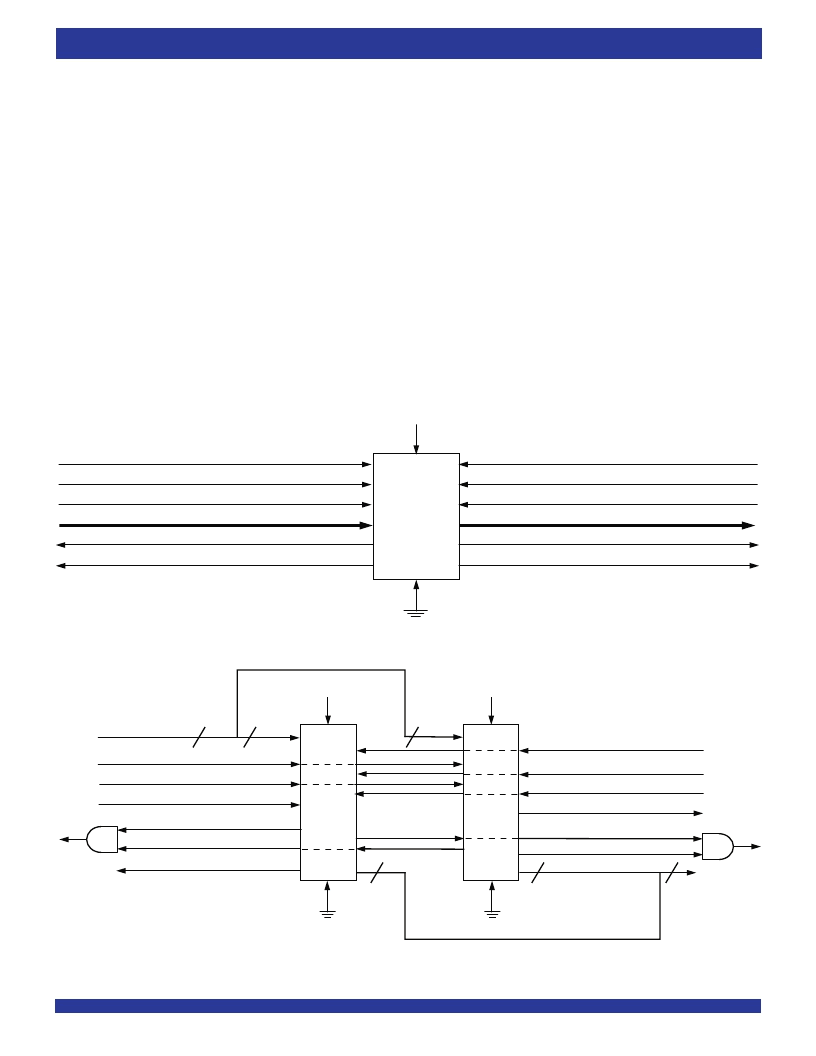
Figure 15. Block Diagram of 64 x 18, 256 x 18, 512 x 18, 1,024 x 18, 2,048 x 18, 4,096 x 18, 8,192 x 18
Synchronous FIFO Used in a Width Expansion Configuration
OPERATING CONFIGURATIONS
SINGLE DEVICE CONFIGURATION
A single IDT72421/72201/72211/72221/72231/72241/72251 may be used
when the application requirements are for 64/256/512/1,024/2,048/4,096/
8,192 words or less. When these FIFOs are in a Single Device Configuration,
the Read Enable 2 (
REN2
) control input can be grounded (see Figure 14). In
this configuration, the Write Enable 2/Load (WEN2/
LD
) pin is set LOW at Reset
so that the pin operates as a control to load and read the programmable flag
offsets.
WIDTH EXPANSION CONFIGURATION
Word width may be increased simply by connecting the corresponding input
controls signals of multiple devices. A composite flag should be created for each
of the endpoint status flags (
EF
and
FF
). The partial status flags (
AE
and
AF
)
can be detected fromany one device. Figure 15 demonstrates a 18-bit word
width by using two IDT72421/72201/72211/72221/72231/72241/72251s.
Any word width can be attained by adding additional IDT72421/72201/72211/
72221/72231/72241/72251s.
When these FIFOs are in a Width Expansion Configuration, the Read
Enable 2 (
REN2
) control input can be grounded (see Figure 15). In this
Figure 14. Block Diagram of Single 64 x 9, 256 x 9, 512 x 9, 1,024 x 9, 2,048 x 9, 4,096 x 9, 8,192 x 9 Synchronous FIFO
DATA OUT (Q
0
- Q
8
)
EMPTY FLAG (
EF
)
DATA IN (D
0
- D
8
)
RESET (
RS
)
READ CLOCK (RCLK)
READ ENABLE 1 (
REN1
)
OUTPUT ENABLE (
OE
)
PROGRAMMABLE ALMOST-EMPTY (
PAE
)
READ ENABLE 2 (
REN2
)
WRITE CLOCK (WCLK)
WRITE ENABLE 1 (
WEN1
)
WRITE ENABLE 2/LOAD (WEN2/
LD
)
FULL FLAG (
FF
)
PROGRAMMABLE ALMOST-FULL (
PAF
)
IDT
72421
72201
72211
72221
72231
72241
72251
2655 drw 16
DATA IN (D)
WRITE CLOCK (WCLK)
18
9
9
RESET (
RS
)
READ CLOCK (RCLK)
DATA OUT (Q)
9
18
READ ENABLE 2 (
REN2
)
READ ENABLE 2 (
REN2
)
WRITE ENABLE1 (
WEN1
)
FULL FLAG (
FF
) #1
FULL FLAG (
FF
) #2
PROGRAMMABLE (
PAF
)
PROGRAMMABLE (
PAE
)
EMPTY FLAG (
EF
) #2
OUTPUT ENABLE (
OE
)
READ ENABLE (
REN
)
9
WRITE ENABLE2/LOAD (WEN2/
LD
)
IDT
72421
72201
72211
72221
72231
72241
72251
EMPTY FLAG (
EF
) #1
RESET (
RS
)
IDT
72421
72201
72211
72221
72231
72241
72251
2655 drw 17
相關(guān)PDF資料 |
PDF描述 |
|---|---|
| IDT72231L15PF | CMOS SyncFIFOO 64 X 9, 256 x 9, 512 x 9, 1024 X 9, 2048 X 9 and 4096 x 9 |
| IDT72231L15PFI | CMOS SyncFIFOO 64 X 9, 256 x 9, 512 x 9, 1024 X 9, 2048 X 9 and 4096 x 9 |
| IDT72201L10JI | CMOS SyncFIFOO 64 X 9, 256 x 9, 512 x 9, 1024 X 9, 2048 X 9 and 4096 x 9 |
| IDT72201L10PF | Dual High Output Current Operational Amplifier 8-TSSOP -40 to 85 |
| IDT72201L10PFI | Dual High Output Current Operational Amplifier 8-TSSOP -40 to 85 |
相關(guān)代理商/技術(shù)參數(shù) |
參數(shù)描述 |
|---|---|
| IDT72231L15JI8 | 功能描述:IC FIFO SYNC 512X9 15NS 32PLCC RoHS:否 類別:集成電路 (IC) >> 邏輯 - FIFO 系列:7200 標(biāo)準(zhǔn)包裝:80 系列:7200 功能:同步 存儲(chǔ)容量:18.4K(1K x 18) 數(shù)據(jù)速率:- 訪問時(shí)間:10ns 電源電壓:4.5 V ~ 5.5 V 工作溫度:0°C ~ 70°C 安裝類型:表面貼裝 封裝/外殼:64-LQFP 供應(yīng)商設(shè)備封裝:64-TQFP(10x10) 包裝:托盤 其它名稱:72225LB10TF |
| IDT72231L15PF | 功能描述:IC FIFO SYNC 512X9 15NS 32QFP RoHS:否 類別:集成電路 (IC) >> 邏輯 - FIFO 系列:7200 標(biāo)準(zhǔn)包裝:80 系列:7200 功能:同步 存儲(chǔ)容量:18.4K(1K x 18) 數(shù)據(jù)速率:- 訪問時(shí)間:10ns 電源電壓:4.5 V ~ 5.5 V 工作溫度:0°C ~ 70°C 安裝類型:表面貼裝 封裝/外殼:64-LQFP 供應(yīng)商設(shè)備封裝:64-TQFP(10x10) 包裝:托盤 其它名稱:72225LB10TF |
| IDT72231L15PF8 | 功能描述:IC FIFO SYNC 512X9 15NS 32QFP RoHS:否 類別:集成電路 (IC) >> 邏輯 - FIFO 系列:7200 標(biāo)準(zhǔn)包裝:80 系列:7200 功能:同步 存儲(chǔ)容量:18.4K(1K x 18) 數(shù)據(jù)速率:- 訪問時(shí)間:10ns 電源電壓:4.5 V ~ 5.5 V 工作溫度:0°C ~ 70°C 安裝類型:表面貼裝 封裝/外殼:64-LQFP 供應(yīng)商設(shè)備封裝:64-TQFP(10x10) 包裝:托盤 其它名稱:72225LB10TF |
| IDT72231L15PFG | 制造商:INTEGRATED DEVICE TECHNOLOGY 功能描述:IC FIFO 2KX9 SMD 72231 TQFP32 |
| IDT72231L15PFGI | 制造商:Integrated Device Technology Inc 功能描述:IC FIFO SYNC 512X9 15NS 32QFP |
發(fā)布緊急采購,3分鐘左右您將得到回復(fù)。