- 您現(xiàn)在的位置:買賣IC網(wǎng) > PDF目錄377405 > IDT72245LB15TFI (INTEGRATED DEVICE TECHNOLOGY INC) CMOS SyncFIFOO 256 x 18, 512 x 18, 1024 x 18, 2048 x 18 and 4096 x 18 PDF資料下載
參數(shù)資料
| 型號(hào): | IDT72245LB15TFI |
| 廠商: | INTEGRATED DEVICE TECHNOLOGY INC |
| 元件分類: | DRAM |
| 英文描述: | CMOS SyncFIFOO 256 x 18, 512 x 18, 1024 x 18, 2048 x 18 and 4096 x 18 |
| 中文描述: | 4K X 18 OTHER FIFO, 10 ns, PQFP64 |
| 封裝: | PLASTIC, STQFP-64 |
| 文件頁(yè)數(shù): | 3/16頁(yè) |
| 文件大小: | 181K |
| 代理商: | IDT72245LB15TFI |
第1頁(yè)第2頁(yè)當(dāng)前第3頁(yè)第4頁(yè)第5頁(yè)第6頁(yè)第7頁(yè)第8頁(yè)第9頁(yè)第10頁(yè)第11頁(yè)第12頁(yè)第13頁(yè)第14頁(yè)第15頁(yè)第16頁(yè)
3
IDT72205LB/72215LB/72225LB/72235LB/72245LB CMOS SyncFIFO
256 x 18-BIT, 512 x 18, 1,024 x 18, 2,048 x 18 and 4,096 x 18
Commercial And Industrial Temperature Ranges
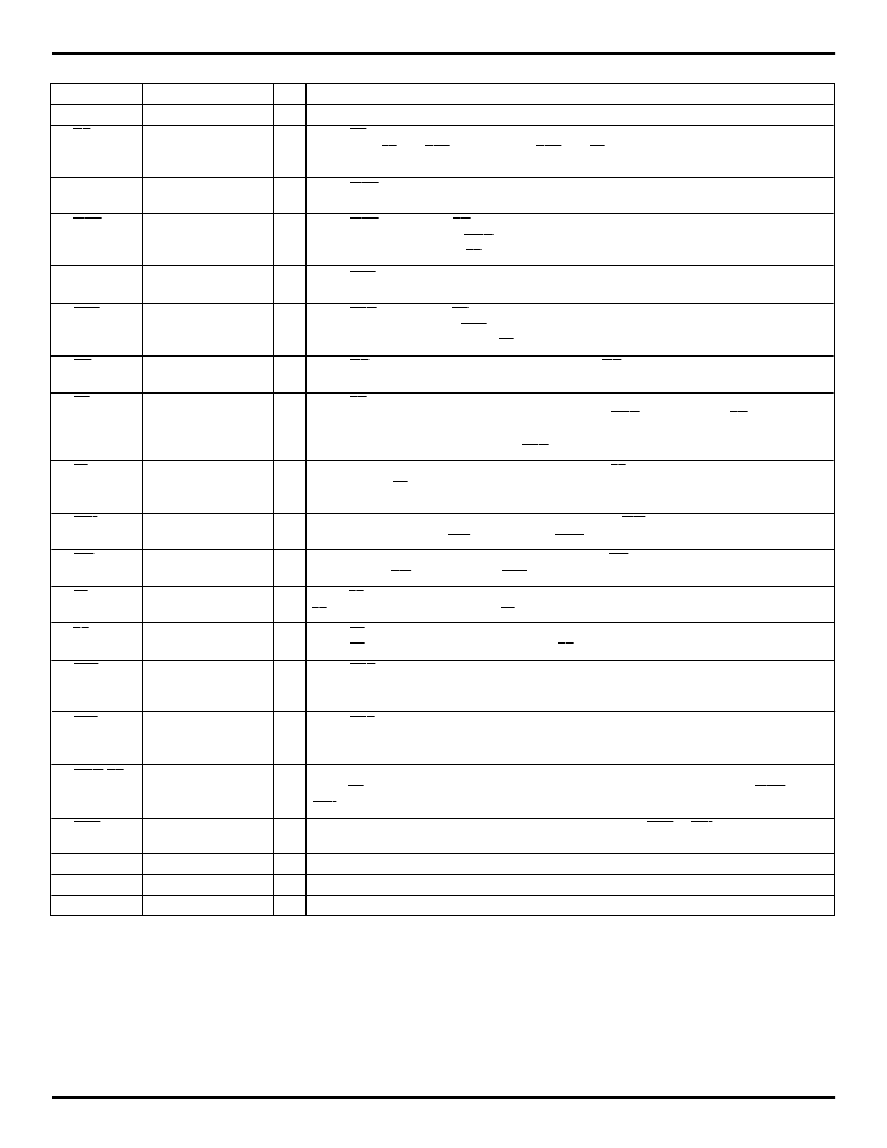
Symbol
D0–D17
RS
Name
I/O
I
I
Description
Data Inputs
Reset
Data inputs for a 18-bit bus.
When
RS
is set LOW, internal read and write pointers are set to the first location of the
RAM array,
FF
and
PAF
go HIGH, and
PAE
and
EF
go LOW. A reset is required before an
initial WRITE after power-up.
When
WEN
is LOW, data is written into the FIFO on a LOW-to-HIGH transition of WCLK,
if the FIFO is not full.
When
WEN
is LOW and
LD
is HIGH, data is written into the FIFO on every LOW-to-HIGH
transition of WCLK. When
WEN
is HIGH, the FIFO holds the previous data. Data will not be
written into the FIFO if the
FF
is LOW.
When
REN
is LOW, data is read from the FIFO on a LOW-to-HIGH transition of RCLK, if the
FIFO is not empty.
When
REN
is LOW and
LD
is HIGH, data is read from the FIFO on every LOW-to-HIGH
transition of RCLK. When
REN
is HIGH, the output register holds the previous data. Data will
not be read from the FIFO if the
EF
is LOW.
When
OE
is LOW, the data output bus is active. If
OE
is HIGH, the output data bus will
be in a high-impedance state.
When
LD
is LOW, data on the inputs D0–D11 is written to the offset and depth registers
on the LOW-to-HIGH transition of the WCLK, when
WEN
is LOW. When
LD
is LOW,
data on the outputs Q0–Q11 is read from the offset and depth registers on the LOW-to-
HIGH transition of the RCLK, when
REN
is LOW.
In the single device or width expansion configuration,
FL
is grounded. In the depth expansion
configuration,
FL
is grounded on the first device (first load device) and set to HIGH for all other
devices in the Daisy Chain.
In the single device or width expansion configuration,
WXI
is grounded. In the
depth
expansion configuration,
WXI
is connected to
WXO
(Write Expansion Out) of the previous device.
In the single device or width expansion configuration,
RXI
is grounded. In the
depth expansion
configuration,
RXI
is connected to
RXO
(Read Expansion Out) of the previous device.
When
FF
is LOW, the FIFO is full and further data writes into the input are inhibited. When
FF
is HIGH, the FIFO is not full.
FF
is synchronized to WCLK.
When
EF
is LOW, the FIFO is empty and further data reads from the output are inhibited.
When
EF
is HIGH, the FIFO is not empty.
EF
is synchronized to RCLK.
When
PAE
is LOW, the FIFO is almost empty based on the offset programmed into the
FIFO. The default offset at reset is 31 from empty for IDT72205LB, 63 from empty for
IDT72215LB, and 127 from empty for IDT72225LB/72235LB/72245LB.
When
PAF
is LOW, the FIFO is almost full based on the offset programmed into the FIFO.
The default offset at reset is 31 from full for IDT72205LB, 63 from full for IDT72215LB, and
127 from full for IDT72225LB/72235LB/72245LB.
In the single device or width expansion configuration, the device is more than half full
when
HF
is LOW. In the depth expansion configuration, a pulse is sent from
WXO
to
WXI
of the next device when the last location in the FIFO is written.
In the depth expansion configuration, a pulse is sent from
RXO
to
RXI
of the next device
when the last location in the FIFO is read.
Data outputs for a 18-bit bus.
+5V power supply pins.
Eight ground pins for the PLCC and seven pins for the TQFP/STQFP.
WCLK
Write Clock
I
WEN
Write Enable
I
RCLK
Read Clock
I
REN
Read Enable
I
OE
Output Enable
I
LD
Load
I
FL
First Load
I
WXI
Write Expansion
I
RXI
Read Expansion
I
FF
Full Flag
O
EF
Empty Flag
O
PAE
Programmable
Almost-Empty Flag
O
PAF
Programmable
Almost-Full Flag
O
WXO
/
HF
Write Expansion
Out/Half-Full Flag
O
RXO
Read Expansion
Out
Data Outputs
Power
Ground
O
Q0–Q17
V
CC
GND
O
PIN DESCRIPTION
相關(guān)PDF資料 |
PDF描述 |
|---|---|
| IDT72245LB20G | CMOS SyncFIFOO 256 x 18, 512 x 18, 1024 x 18, 2048 x 18 and 4096 x 18 |
| IDT72245LB20GB | CMOS SyncFIFOO 256 x 18, 512 x 18, 1024 x 18, 2048 x 18 and 4096 x 18 |
| IDT72215LB | CMOS SyncFIFOO 256 x 18, 512 x 18, 1024 x 18, 2048 x 18 and 4096 x 18 |
| IDT72215LB10TF | CMOS SyncFIFOO 256 x 18, 512 x 18, 1024 x 18, 2048 x 18 and 4096 x 18 |
| IDT72215LB10TFI | CMOS SyncFIFOO 256 x 18, 512 x 18, 1024 x 18, 2048 x 18 and 4096 x 18 |
相關(guān)代理商/技術(shù)參數(shù) |
參數(shù)描述 |
|---|---|
| IDT72245LB15TFI8 | 功能描述:IC FIFO 1024X18 SYNC 15NS 64QFP RoHS:否 類別:集成電路 (IC) >> 邏輯 - FIFO 系列:7200 標(biāo)準(zhǔn)包裝:90 系列:7200 功能:同步 存儲(chǔ)容量:288K(16K x 18) 數(shù)據(jù)速率:100MHz 訪問(wèn)時(shí)間:10ns 電源電壓:4.5 V ~ 5.5 V 工作溫度:0°C ~ 70°C 安裝類型:表面貼裝 封裝/外殼:64-LQFP 供應(yīng)商設(shè)備封裝:64-TQFP(14x14) 包裝:托盤 其它名稱:72271LA10PF |
| IDT72245LB25J | 功能描述:IC FIFO 1024X18 SYNC 25NS 68PLCC RoHS:否 類別:集成電路 (IC) >> 邏輯 - FIFO 系列:7200 標(biāo)準(zhǔn)包裝:80 系列:7200 功能:同步 存儲(chǔ)容量:18.4K(1K x 18) 數(shù)據(jù)速率:- 訪問(wèn)時(shí)間:10ns 電源電壓:4.5 V ~ 5.5 V 工作溫度:0°C ~ 70°C 安裝類型:表面貼裝 封裝/外殼:64-LQFP 供應(yīng)商設(shè)備封裝:64-TQFP(10x10) 包裝:托盤 其它名稱:72225LB10TF |
| IDT72245LB25J8 | 功能描述:IC FIFO 1024X18 SYNC 25NS 68PLCC RoHS:否 類別:集成電路 (IC) >> 邏輯 - FIFO 系列:7200 標(biāo)準(zhǔn)包裝:80 系列:7200 功能:同步 存儲(chǔ)容量:18.4K(1K x 18) 數(shù)據(jù)速率:- 訪問(wèn)時(shí)間:10ns 電源電壓:4.5 V ~ 5.5 V 工作溫度:0°C ~ 70°C 安裝類型:表面貼裝 封裝/外殼:64-LQFP 供應(yīng)商設(shè)備封裝:64-TQFP(10x10) 包裝:托盤 其它名稱:72225LB10TF |
| IDT72245LB25JI | 功能描述:IC FIFO 1024X18 SYNC 25NS 68PLCC RoHS:否 類別:集成電路 (IC) >> 邏輯 - FIFO 系列:7200 標(biāo)準(zhǔn)包裝:90 系列:7200 功能:同步 存儲(chǔ)容量:288K(16K x 18) 數(shù)據(jù)速率:100MHz 訪問(wèn)時(shí)間:10ns 電源電壓:4.5 V ~ 5.5 V 工作溫度:0°C ~ 70°C 安裝類型:表面貼裝 封裝/外殼:64-LQFP 供應(yīng)商設(shè)備封裝:64-TQFP(14x14) 包裝:托盤 其它名稱:72271LA10PF |
| IDT72245LB25JI8 | 功能描述:IC FIFO 1024X18 SYNC 25NS 68PLCC RoHS:否 類別:集成電路 (IC) >> 邏輯 - FIFO 系列:7200 標(biāo)準(zhǔn)包裝:80 系列:7200 功能:同步 存儲(chǔ)容量:18.4K(1K x 18) 數(shù)據(jù)速率:- 訪問(wèn)時(shí)間:10ns 電源電壓:4.5 V ~ 5.5 V 工作溫度:0°C ~ 70°C 安裝類型:表面貼裝 封裝/外殼:64-LQFP 供應(yīng)商設(shè)備封裝:64-TQFP(10x10) 包裝:托盤 其它名稱:72225LB10TF |
發(fā)布緊急采購(gòu),3分鐘左右您將得到回復(fù)。