- 您現(xiàn)在的位置:買賣IC網(wǎng) > PDF目錄377419 > IDT72401L45SOB (Integrated Device Technology, Inc.) CMOS PARALLEL FIFO 64 x 4-BIT AND 64 x 5-BIT PDF資料下載
參數(shù)資料
| 型號(hào): | IDT72401L45SOB |
| 廠商: | Integrated Device Technology, Inc. |
| 英文描述: | CMOS PARALLEL FIFO 64 x 4-BIT AND 64 x 5-BIT |
| 中文描述: | CMOS并行FIFO的64 × 4位和64 × 5位 |
| 文件頁數(shù): | 1/9頁 |
| 文件大小: | 95K |
| 代理商: | IDT72401L45SOB |
Integrated Device Technology, Inc.
MILITARY AND COMMERCIAL TEMPERATURE RANGES
SEPTEMBER 1996
1996 Integrated Device Technology, Inc.
DSC-2747/7
5.01
1
FEATURES:
First-ln/First-Out Dual-Port memory
64 x 4 organization (IDT72401/03)
64 x 5 organization (IDT72402/04)
IDT72401/02 pin and functionally compatible with
MMI67401/02
RAM-based FIFO with low falI-through time
Low-power consumption
— Active: 175mW (typ.)
Maximum shift rate — 45MHz
High data output drive capability
Asynchronous and simultaneous read and write
Fully expandable by bit width
Fully expandable by word depth
IDT72403/04 have Output Enable pin to enable output
data
High-speed data communications applications
High-performance CMOS technology
Available in CERDIP, plastic DIP and SOIC
Military product compliant to MlL-STD-883, Class B
Standard Military Drawing #5962-86846 and
5962-89523 is listed on this function.
Industrial temperature range (–40
°
C to +85
°
C) is avail-
able, tested to military electrical specifications
DESCRIPTION:
The IDT72401 and IDT72403 are asynchronous high-
performance First-ln/First-Out memories organized 64 words
by 4 bits. The IDT72402 and IDT72404 are asynchronous
high-performance First-ln/First-Out memories organized as
64 words by 5 bits. The IDT72403 and IDT72404 also have an
Output Enable (
OE
) pin. The FlFOs accept 4-bit or 5-bit data
at the data input (D
0-D3, 4
). The stored data stack up on a first-
in/first-out basis.
A Shift Out (SO) signal causes the data at the next to last
word to be shifted to the output while all other data shifts down
one location in the stack. The Input Ready (IR) signal acts like
a flag to indicate when the input is ready for new data
(IR = HIGH) or to signal when the FIFO is full (IR = LOW). The
Input Ready signal can also be used to cascade multiple
devices together. The Output Ready (OR) signal is a flag to
indicate that the output remains valid data (OR = HIGH) or to
indicate that the FIFO is empty (OR = LOW). The Output
Ready can also be used to cascade multiple devices together.
Width expansion is accomplished by logically ANDing the
Input Ready (IR) and Output Ready (OR) signals to form
composite signals.
Depth expansion is accomplished by tying the data inputs
of one device to the data outputs of the previous device. The
Input Ready pin of the receiving device is connected to the
Shift Out pin of the sending device and the Output Ready pin
of the sending device is connected to the Shift In pin of the
receiving device.
Reading and writing operations are completely asynchro-
nous allowing the FIFO to be used as a buffer between two
digital machines of widely varying operating frequencies. The
45MHz speed makes these FlFOs ideal for high-speed
communication and controller applications.
Military grade product is manufactured in compliance with
the latest revision of MIL-STD-883, Class B.
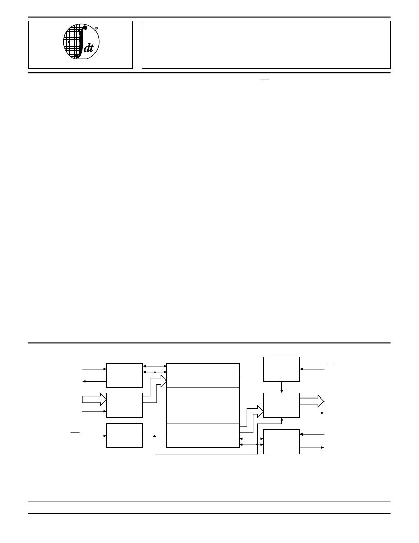
IDT72401
IDT72402
IDT72403
IDT72404
CMOS PARALLEL FIFO
64 x 4-BIT AND 64 x 5-BIT
D
0-3
2747 drw 01
INPUT
CONTROL
LOGIC
DATA
MASTER
RESET
IN
WRITE POINTER
WRITE MULTIPLEXER
MEMORY
ARRAY
READ MULTIPLEXER
READ POINTER
OUTPUT
ENABLE
DATA
OUTPUT
CONTROL
LOGIC
OUT
SI
IR
D
4
(IDT72402
and IDT72404)
MR
OE (IDT72403 and
IDT72404)
Q
0-3
Q
4
(IDT72402 and
IDT72404)
SO
OR
The IDT logo is a registered trademark of Integrated Device Technology, Inc.
FAST is a trademark of National Semiconductor, Inc.
For latest information contact IDT's web site at www.idt.com or fax-on-demand at 408-492-8391.
FUNCTIONAL BLOCK DIAGRAM
相關(guān)PDF資料 |
PDF描述 |
|---|---|
| IDT72402 | Current-Mode PWM Controller 14-SOIC 0 to 70 |
| IDT72403 | Current-Mode PWM Controller 8-SOIC 0 to 70 |
| IDT72403L10D | Current-Mode PWM Controller 14-SOIC 0 to 70 |
| IDT72403L10DB | Current-Mode PWM Controller 8-SOIC 0 to 70 |
| IDT72403L10P | CMOS PARALLEL FIFO 64 x 4-BIT AND 64 x 5-BIT |
相關(guān)代理商/技術(shù)參數(shù) |
參數(shù)描述 |
|---|---|
| IDT72401L45SOG | 功能描述:IC FIFO 64X4 PAR 45NS 16SOIC RoHS:是 類別:集成電路 (IC) >> 邏輯 - FIFO 系列:7200 標(biāo)準(zhǔn)包裝:80 系列:7200 功能:同步 存儲(chǔ)容量:18.4K(1K x 18) 數(shù)據(jù)速率:- 訪問時(shí)間:10ns 電源電壓:4.5 V ~ 5.5 V 工作溫度:0°C ~ 70°C 安裝類型:表面貼裝 封裝/外殼:64-LQFP 供應(yīng)商設(shè)備封裝:64-TQFP(10x10) 包裝:托盤 其它名稱:72225LB10TF |
| IDT72401L45SOG8 | 制造商:Integrated Device Technology Inc 功能描述:IC FIFO PAR 64X4 45NS 16-SOIC |
| IDT72403L10DB | 制造商:Integrated Device Technology Inc 功能描述:IC FIFO ASYNC 64X4 10NS 16CDIP |
| IDT72403L10P | 功能描述:IC FIFO PAR 64X4 10NS 16-DIP RoHS:否 類別:集成電路 (IC) >> 邏輯 - FIFO 系列:7200 標(biāo)準(zhǔn)包裝:80 系列:7200 功能:同步 存儲(chǔ)容量:18.4K(1K x 18) 數(shù)據(jù)速率:- 訪問時(shí)間:10ns 電源電壓:4.5 V ~ 5.5 V 工作溫度:0°C ~ 70°C 安裝類型:表面貼裝 封裝/外殼:64-LQFP 供應(yīng)商設(shè)備封裝:64-TQFP(10x10) 包裝:托盤 其它名稱:72225LB10TF |
| IDT72403L10SO | 功能描述:IC FIFO PAR 64X4 10NS 16-SOIC RoHS:否 類別:集成電路 (IC) >> 邏輯 - FIFO 系列:7200 標(biāo)準(zhǔn)包裝:80 系列:7200 功能:同步 存儲(chǔ)容量:18.4K(1K x 18) 數(shù)據(jù)速率:- 訪問時(shí)間:10ns 電源電壓:4.5 V ~ 5.5 V 工作溫度:0°C ~ 70°C 安裝類型:表面貼裝 封裝/外殼:64-LQFP 供應(yīng)商設(shè)備封裝:64-TQFP(10x10) 包裝:托盤 其它名稱:72225LB10TF |
發(fā)布緊急采購,3分鐘左右您將得到回復(fù)。