- 您現(xiàn)在的位置:買賣IC網(wǎng) > PDF目錄377189 > IDT74FCT273CT (Integrated Device Technology, Inc.) FAST CMOS OCTAL D FLIP-FLOP WITH MASTER RESET PDF資料下載
參數(shù)資料
| 型號(hào): | IDT74FCT273CT |
| 廠商: | Integrated Device Technology, Inc. |
| 英文描述: | FAST CMOS OCTAL D FLIP-FLOP WITH MASTER RESET |
| 中文描述: | 快速CMOS八路D觸發(fā)器與主復(fù)位次浮點(diǎn)運(yùn)算 |
| 文件頁(yè)數(shù): | 1/7頁(yè) |
| 文件大小: | 109K |
| 代理商: | IDT74FCT273CT |
Integrated Device Technology, Inc.
FAST CMOS
OCTAL D FLIP-FLOP
WITH MASTER RESET
IDT54/74FCT273T/AT/CT
DESCRIPTION:
The IDT54/74FCT273T/AT/CT are octal D flip-flops built
using an advanced dual metal CMOS technology. The IDT54/
74FCT273T/AT/CT have eight edge-triggered D-type flip-
flops with individual D inputs and O outputs. The common
buffered Clock (CP) and Master Reset (
MR
) inputs load and
reset (clear) all flip-flops simultaneously.
The register is fully edge-triggered. The state of each D
input, one set-up time before the LOW-to-HIGH clock
transition, is transferred to the corresponding flip-flop’s O
output.
All outputs will be forced LOW independently of Clock or
Data inputs by a LOW voltage level on the
MR
input. The
device is useful for applications where the true output only is
required and the Clock and Master Reset are common to all
storage elements.
PIN CONFIGURATIONS
INDEX
D
1
O
1
O
2
D
2
D
3
D
7
D
6
O
6
O
5
D
5
O
0
D
0
M
V
C
O
7
O
3
G
C
O
4
D
4
LCC
TOP VIEW
3
2
20 19
1
4
5
6
7
8
18
17
16
15
14
9 10 11 12 13
L20-2
2568 drw 01
2568 drw 02
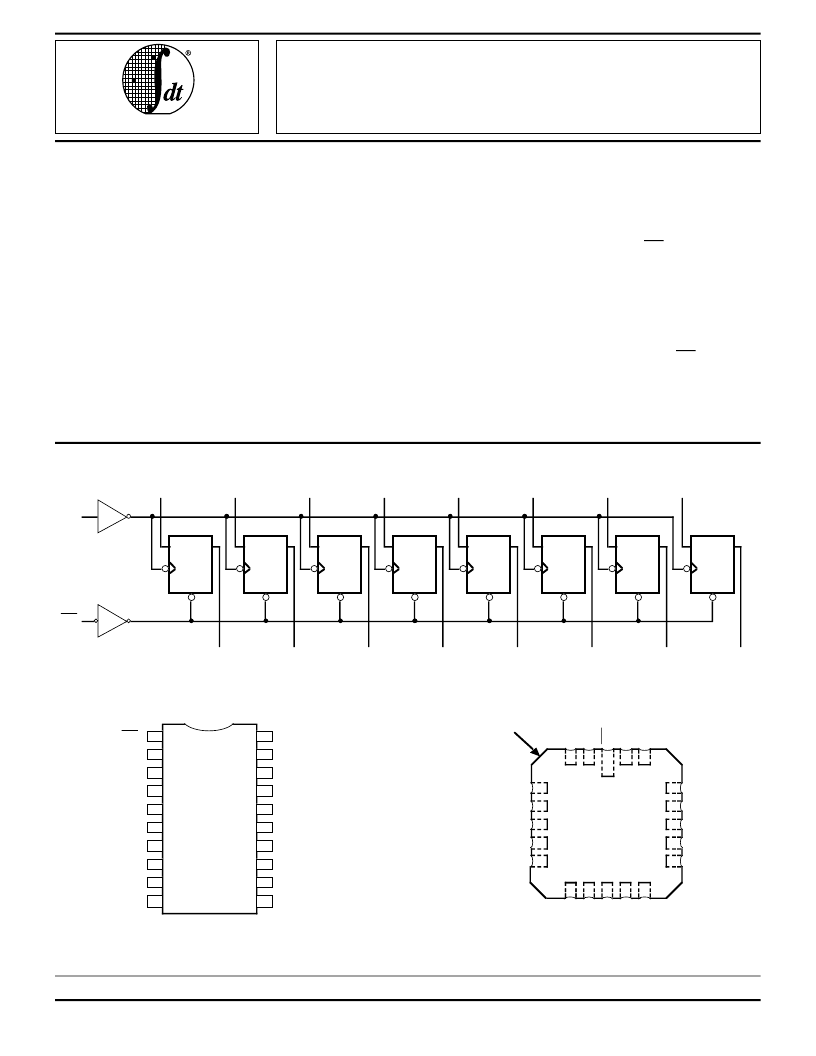
FUNCTIONAL BLOCK DIAGRAM
D
CP
R
D
Q
D
CP
R
D
Q
O
0
O
1
O
2
O
3
O
4
O
5
O
6
O
7
CP
MR
D
CP
R
D
Q
D
CP
R
D
Q
D
CP
R
D
Q
D
CP
R
D
Q
D
CP
R
D
Q
D
CP
R
D
Q
D
0
D
1
D
2
D
3
D
4
D
5
D
6
D
7
2568 drw 03
MILITARY AND COMMERCIAL TEMPERATURE RANGES
APRIL 1995
1995 Integrated Device Technology, Inc.
6.10
DSC-4209/3
1
The IDT logo is a registered trademark of Integrated Device Technology, Inc.
FEATURES:
Std., A, and C speed grades
Low input and output leakage
≤
1
μ
A (max.)
CMOS power levels
True TTL input and output compatibility
– V
OH
= 3.3V (typ.)
– V
OL
= 0.3V (typ.)
High drive outputs (-15mA I
OH
, 48mA I
OL
)
Meets or exceeds JEDEC standard 18 specifications
Product available in Radiation Tolerant and Radiation
Enhanced versions
Military product compliant to MIL-STD-883, Class B
and DESC listed (dual marked)
Available in DIP, SOIC, QSOP, CERPACK and LCC
packages
MR
O
0
D
0
D
1
O
1
O
2
D
2
D
3
O
3
GND
O
7
D
7
D
6
O
6
O
5
D
5
D
4
O
4
CP
V
CC
1
2
3
4
5
6
7
8
9
10
11
12
13
14
15
16
17
18
19
20
DIP/SOIC/QSOP/CERPACK
TOP VIEW
P20-1
D20-1
SO20-2
SO20-8
&
E20-1
相關(guān)PDF資料 |
PDF描述 |
|---|---|
| IDT74FCT273CTD | FAST CMOS OCTAL D FLIP-FLOP WITH MASTER RESET |
| IDT74FCT273CTDB | FAST CMOS OCTAL D FLIP-FLOP WITH MASTER RESET |
| IDT74FCT273CTE | FAST CMOS OCTAL D FLIP-FLOP WITH MASTER RESET |
| IDT74FCT273CTEB | FAST CMOS OCTAL D FLIP-FLOP WITH MASTER RESET |
| IDT74FCT273CTL | FAST CMOS OCTAL D FLIP-FLOP WITH MASTER RESET |
相關(guān)代理商/技術(shù)參數(shù) |
參數(shù)描述 |
|---|---|
| IDT74FCT273HTP | 制造商:Rochester Electronics LLC 功能描述:- Bulk |
| IDT74FCT273P | 制造商:Integrated Device Technology Inc 功能描述: |
| IDT74FCT273TP | 制造商:Integrated Device Technology Inc 功能描述: |
| IDT74FCT273TPY | 制造商:Rochester Electronics LLC 功能描述:- Bulk |
| IDT74FCT273TQ | 制造商:Rochester Electronics LLC 功能描述:- Bulk |
發(fā)布緊急采購(gòu),3分鐘左右您將得到回復(fù)。