- 您現(xiàn)在的位置:買賣IC網(wǎng) > PDF目錄377233 > IDT74FCT827ATSOB (Integrated Device Technology, Inc.) FAST CMOS 10-BIT BUFFERS PDF資料下載
參數(shù)資料
| 型號: | IDT74FCT827ATSOB |
| 廠商: | Integrated Device Technology, Inc. |
| 英文描述: | FAST CMOS 10-BIT BUFFERS |
| 中文描述: | 快速CMOS 10位緩沖器 |
| 文件頁數(shù): | 2/7頁 |
| 文件大小: | 127K |
| 代理商: | IDT74FCT827ATSOB |
IDT54/74FCT827AT/BT/CT/DT, IDT54/74FCT2827AT/BT/CT
HIGH-PERFORMANCE CMOS BUFFERS
MILITARY AND COMMERCIAL TEMPERATURE RANGES
6.22
2
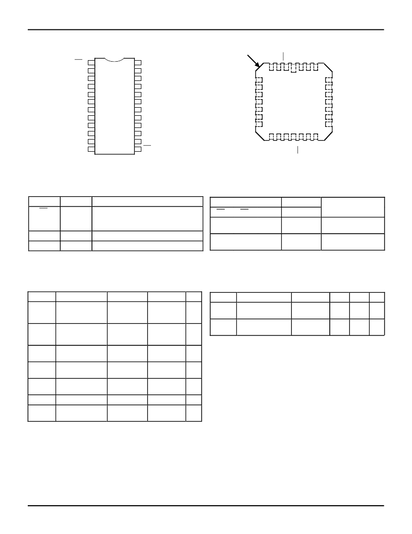
PIN CONFIGURATIONS
DIP/SOIC/SSOP/QSOP/CERPACK
TOP VIEW
2573 drw 02
2573 drw 03
LCC
TOP VIEW
OE
1
D
0
D
1
D
2
D
3
D
4
D
5
D
6
D
7
D
8
D
9
GND
Y
0
Y
1
Y
2
Y
3
Y
4
Y
5
Y
6
Y
7
Y
8
Y
9
OE
2
V
CC
1
2
3
4
5
6
7
8
9
10
11
12
13
14
15
16
17
18
19
20
P24-1
D24-1
SO24-2
SO24-7
SO24-8
&
E24-1
21
22
23
24
INDEX
D
2
D
3
D
4
NC
D
5
D
6
D
7
Y
2
Y
3
Y
4
NC
Y
5
Y
6
Y
7
O
1
D
1
N
V
C
Y
0
D
8
G
O
2
Y
9
Y
8
3 2
20
19
1
4
5
6
7
8
9
10
11
18
17
16
15
14
1213
L28-1
D
0
Y
1
21
22
23
24
25
26
27
28
D
9
N
PIN DESCRIPTION
2573 tbl 01
Names
OE
I
I/O
I
Description
When both are LOW the outputs are
enabled. When either one or both are
HIGH the outputs are High Z.
10-bit data input.
10-bit data output.
D
I
Y
I
I
O
CAPACITANCE
(T
A
= +25
°
C, f = 1.0MHz)
Symbol
Parameter
(1)
C
IN
Input
Capacitance
C
OUT
Output
Capacitance
NOTE:
1. This parameter is measured at characterization but not tested.
ABSOLUTE MAXIMUM RATINGS
(1)
Symbol
Rating
V
TERM(2)
Terminal Voltage
with Respect to
GND
V
TERM(3)
Terminal Voltage
with Respect to
GND
T
A
Operating
Temperature
T
BIAS
Temperature
Under Bias
T
STG
Storage
Temperature
P
T
Power Dissipation
Commercial
–0.5 to +7.0
Military
–0.5 to +7.0
Unit
V
–0.5 to
V
CC
+0.5
–0.5 to
V
CC
+0.5
V
0 to +70
–55 to +125
°
C
–55 to +125
–65 to +135
°
C
–55 to +125
–65 to +150
°
C
0.5
0.5
W
I
OUT
DC Output
Current
–60 to +120 –60 to +120 mA
NOTES:
1. Stresses greater than those listed under ABSOLUTE MAXIMUM RAT-
INGS may cause permanent damage to the device. This is a stress rating
only and functional operation of the device at these or any other conditions
above those indicated in the operational sections of this specification is
not
implied. Exposure to absolute maximum rating conditions for
extended periods may affect reliability. No terminal voltage may exceed
V
CC
by +0.5V unless otherwise noted.
2. Input and V
CC
terminals only.
3. Outputs and I/O terminals only.
2573 lnk 03
Conditions
V
IN
= 0V
Typ.
6
Max. Unit
10
pF
V
OUT
= 0V
8
12
pF
2573 lnk 04
Inputs
Output
OE
1
OE
2
D
I
L
H
X
X
Y
I
L
H
Z
Z
Function
Transparent
L
L
H
X
L
L
X
H
Three-State
NOTE
:
1. H = HIGH, L = LOW, X = Don’t Care, Z = High Impedance
2573 tbl 02
FUNCTION TABLE
(1)
相關PDF資料 |
PDF描述 |
|---|---|
| IDT74FCT827DT | FAST CMOS 10-BIT BUFFERS |
| IDT74FCT827DTD | FAST CMOS 10-BIT BUFFERS |
| IDT74FCT827DTDB | FAST CMOS 10-BIT BUFFERS |
| IDT74FCT827DTE | FAST CMOS 10-BIT BUFFERS |
| IDT74FCT827DTEB | FAST CMOS 10-BIT BUFFERS |
相關代理商/技術參數(shù) |
參數(shù)描述 |
|---|---|
| IDT74FCT827BTPY | 制造商:Rochester Electronics LLC 功能描述:- Bulk 制造商:Integrated Device Technology Inc 功能描述: |
| IDT74FCT827CTP | 制造商:Integrated Device Technology Inc 功能描述: |
| IDT74FCT827CTSO | 制造商:Integrated Device Technology Inc 功能描述: |
| IDT74FCT827HBP | 制造商:Rochester Electronics LLC 功能描述:- Bulk |
| IDT74FCT827HCTP | 制造商:Rochester Electronics LLC 功能描述:- Bulk |
發(fā)布緊急采購,3分鐘左右您將得到回復。