- 您現(xiàn)在的位置:買賣IC網(wǎng) > PDF目錄377236 > IDT74FCT841DTQB (Integrated Device Technology, Inc.) FAST CMOS BUS INTERFACE LATCHES PDF資料下載
參數(shù)資料
| 型號: | IDT74FCT841DTQB |
| 廠商: | Integrated Device Technology, Inc. |
| 英文描述: | FAST CMOS BUS INTERFACE LATCHES |
| 中文描述: | 快速CMOS總線接口鎖存 |
| 文件頁數(shù): | 5/7頁 |
| 文件大?。?/td> | 138K |
| 代理商: | IDT74FCT841DTQB |
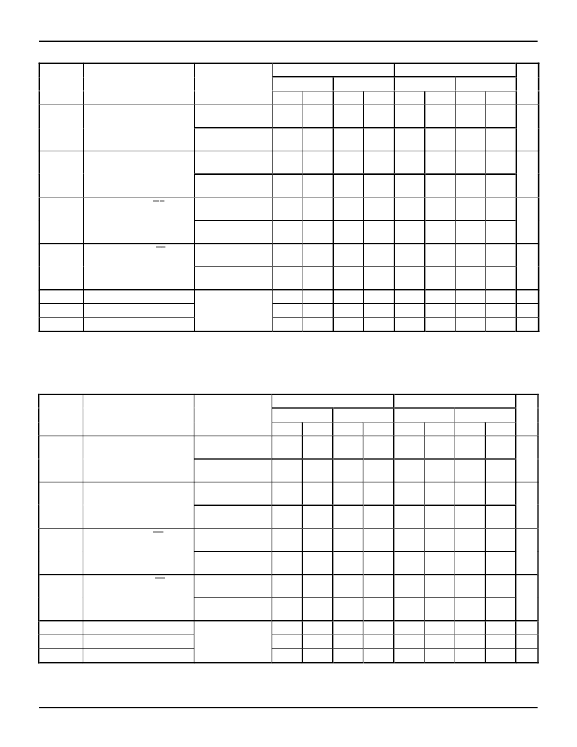
6.22
5
IDT54/74FCT841AT/BT/CT/DT
FAST CMOS BUS INTERFACE LATCHES
MILITARY AND COMMERCIAL TEMPERATURE RANGES
SWITCHING CHARACTERISTICS OVER OPERATING RANGE
SWITCHING CHARACTERISTICS OVER OPERATING RANGE
FCT841AT
FCT841BT
Com'l.
Mil.
Com'l.
Mil.
Symbol
t
PLH
t
PHL
Parameter
Conditions
(1)
C
L
= 50pF
R
L
= 500
C
L
= 300pF
(4)
R
L
= 500
C
L
= 50pF
R
L
= 500
C
L
= 300pF
(4)
R
L
= 500
C
L
= 50pF
R
L
= 500
C
L
= 300pF
(4)
R
L
= 500
C
L
= 5pF
(4)
R
L
= 500
C
L
= 50pF
R
L
= 500
C
L
= 50pF
R
L
= 500
Min.
(2)
1.5
Max.
9.0
Min.
(2)
1.5
Max.
10.0
Min.
(2)
1.5
Max.
6.5
Min.
(2)
1.5
Max.
7.5
Unit
ns
Propagation Delay
D
I
to Y
I
(LE = HIGH)
1.5
13.0
1.5
15.0
1.5
13.0
1.5
15.0
t
PLH
t
PHL
Propagation Delay
LE to Y
I
1.5
12.0
1.5
13.0
1.5
8.0
1.5
10.5
ns
1.5
16.0
1.5
20.0
1.5
15.5
1.5
18.0
t
PZH
t
PZL
Output Enable Time
OE
to Y
I
1.5
11.5
1.5
13.0
1.5
8.0
1.5
8.5
ns
1.5
23.0
1.5
25.0
1.5
14.0
1.5
15.0
t
PHZ
t
PLZ
Output Disable Time
OE
to Y
I
1.5
7.0
1.5
9.0
1.5
6.0
1.5
6.5
ns
1.5
8.0
1.5
10.0
1.5
7.0
1.5
7.5
t
SU
t
H
t
W
Data to LE Set-up Time
2.5
2.5
4.0
—
—
—
2.5
3.0
5.0
—
—
—
2.5
2.5
4.0
—
—
—
2.5
2.5
4.0
—
—
—
ns
ns
ns
Data to LE Hold Time
LE Pulse Width HIGH
(3)
NOTES:
1. See test circuit and waveforms.
2. Minimum limits are guaranteed but not tested on Propagation Delays.
2571 tbl 08
3. These parameters are guaranteed but not tested.
4. These conditions are guaranteed but not tested.
FCT841CT
FCT841DT
Com'l.
Mil.
Com'l.
Mil.
Symbol
t
PLH
t
PHL
Parameter
Conditions
(1)
C
L
= 50pF
R
L
= 500
C
L
= 300pF
(4)
R
L
= 500
C
L
= 50pF
R
L
= 500
C
L
= 300pF
(4)
R
L
= 500
C
L
= 50pF
R
L
= 500
C
L
= 300pF
(4)
R
L
= 500
C
L
= 5pF
(4)
R
L
= 500
C
L
= 50pF
R
L
= 500
C
L
= 50pF
R
L
= 500
Min.
(2)
1.5
Max.
5.5
Min.
(2)
1.5
Max.
6.3
Min.
(2)
1.5
Max.
4.2
Min.
(2)
—
Max.
—
Unit
ns
Propagation Delay
D
I
to Y
I
(LE = HIGH)
1.5
13.0
1.5
15.0
1.5
8.0
—
—
t
PLH
t
PHL
Propagation Delay
LE to Y
I
1.5
6.4
1.5
6.8
1.5
4.0
—
—
ns
1.5
15.0
1.5
16.0
1.5
8.0
—
—
t
PZH
t
PZL
Output Enable Time
OE
to Y
I
1.5
6.5
1.5
7.3
1.5
4.8
—
—
ns
1.5
12.0
1.5
13.0
1.5
9.0
—
—
t
PHZ
t
PLZ
Output Disable Time
OE
to Y
I
1.5
5.7
1.5
6.0
1.5
4.0
—
—
ns
1.5
6.0
1.5
6.3
1.5
4.0
—
—
t
SU
t
H
t
W
Data to LE Set-up Time
2.5
2.5
4.0
—
—
—
2.5
2.5
4.0
—
—
—
1.5
1.0
3.0
—
—
—
—
—
—
—
—
—
ns
ns
ns
Data to LE Hold Time
LE Pulse Width HIGH
(3)
NOTES:
1. See test circuit and waveforms.
2. Minimum limits are guaranteed but not tested on Propagation Delays.
2571 tbl 09
3. These parameters are guaranteed but not tested.
4. These conditions are guaranteed but not tested.
相關(guān)PDF資料 |
PDF描述 |
|---|---|
| IDT74FCT841DTSO | FAST CMOS BUS INTERFACE LATCHES |
| IDT74FCT841DTSOB | FAST CMOS BUS INTERFACE LATCHES |
| IDT54FCT841BTPY | FAST CMOS BUS INTERFACE LATCHES |
| IDT54FCT841BTPYB | FAST CMOS BUS INTERFACE LATCHES |
| IDT54FCT841BTQ | FAST CMOS BUS INTERFACE LATCHES |
相關(guān)代理商/技術(shù)參數(shù) |
參數(shù)描述 |
|---|---|
| IDT74FCT841HAP | 制造商:Rochester Electronics LLC 功能描述:- Bulk |
| IDT74FCT841HATP | 制造商:Integrated Device Technology Inc 功能描述: |
| IDT74FCT841HBP | 制造商:Integrated Device Technology Inc 功能描述: |
| IDT74FCT88915T55J | 制造商:Integrated Device Technology Inc 功能描述: |
| IDT74FCT88915TT100J | 制造商:Integrated Device Technology Inc 功能描述: |
發(fā)布緊急采購,3分鐘左右您將得到回復(fù)。