- 您現(xiàn)在的位置:買賣IC網(wǎng) > PDF目錄360829 > IDTQS74FCT2574ATQ Buffer/Driver PDF資料下載
參數(shù)資料
| 型號(hào): | IDTQS74FCT2574ATQ |
| 元件分類: | 通用總線功能 |
| 英文描述: | Buffer/Driver |
| 中文描述: | 緩沖器/驅(qū)動(dòng)器 |
| 文件頁(yè)數(shù): | 2/6頁(yè) |
| 文件大小: | 117K |
| 代理商: | IDTQS74FCT2574ATQ |
2
INDUSTRIAL TEMPERATURE RANGE
IDTQS74FCT153AT/CT
HIGH-SPEED CMOS DUAL 4-INPUT MULTIPLEXER
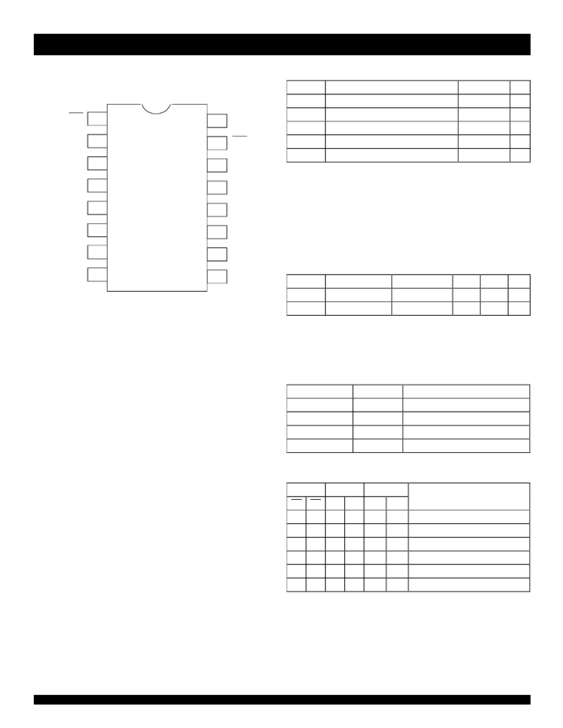
PIN CONFIGURATION
SOIC/ QSOP
TOP VIEW
SO16-1
SO16-7
2
3
4
5
6
7
8
9
10
11
12
13
14
15
16
1
EA
S
1
GND
YA
I
1A
I
0A
I
3A
EB
S
0
I
3B
I
2B
I
1B
I
0B
YB
V
CC
I
2A
ABSOLUTE MAXIMUM RATINGS
(1)
Symbol
V
TERM
T
STG
I
OUT
I
IK
I
OK
Description
Max.
Unit
V
°C
mA
mA
mA
FCTL
Termnal Voltage with Respect to GND
Storage Temperature
DC Output Current Max Sink Current/Pin
Input Diode Current, V
IN
< 0
Output Diode Current, V
OUT
< 0
– 0.5 to +7
– 65 to +150
120
– 20
– 50
NOTE:
1. Stresses greater than those listed under ABSOLUTE MAXIMUM
RATINGS may cause permanent damage to the device. This is a
stress rating only and functional operation of the device at these or
any other conditions above those indicated in the operational sections
of this specification is not implied. Exposure to absolute maximum
rating conditions for extended periods may affect reliability.
CAPACITANCE
(T
A
= +25
O
C, f = 1.0MHz)
Parameter
(1)
C
IN
Input Capacitance
C
OUT
Output Capacitance
Symbol
Conditions
V
IN
= 0V
V
OUT
= 0V
Typ.
4
8
Max.
—
—
Unit
pF
pF
FCT_2
NOTE:
1. This parameter is measured at characterization but not tested.
PIN DESCRIPTION
Pin Names
I
0
- I
7
S
0
- S
1
EA
,
EB
YA, YB
I/O
I
I
I
0
Description
Data In
Select
Enable
Data Out
FUNCTION TABLE
(1)
Enable
Select
Outputs
EA
H
X
L
L
L
L
EB
X
H
L
L
L
L
S1
X
X
L
L
H
H
S0
X
X
L
H
L
H
YA
L
X
I
0
A
I
1
A
I
2
A
I
3
A
YB
X
L
I
0
B
I
1
B
I
2
B
I
3
B
Function
Disable A
Disable B
S
1
- 0 = 0
S
1
- 0 = 1
S
1
- 0 = 2
S
1
- 0 = 3
NOTE:
1. H = HIGH Voltage Level
L = LOW Voltage Level
X = Don’t Care
相關(guān)PDF資料 |
PDF描述 |
|---|---|
| IDTQS74FCT2574ATSO | Buffer/Driver |
| IDTQS74FCT2574CTQ | Buffer/Driver |
| IDTQS74FCT2574CTSO | Buffer/Driver |
| IDTQS74FCT2574TQ | Buffer/Driver |
| IDTQS74FCT2574TSO | Buffer/Driver |
相關(guān)代理商/技術(shù)參數(shù) |
參數(shù)描述 |
|---|---|
| IDTQS74FCT2574ATSO | 制造商:未知廠家 制造商全稱:未知廠家 功能描述:Buffer/Driver |
| IDTQS74FCT2574CTQ | 制造商:未知廠家 制造商全稱:未知廠家 功能描述:Buffer/Driver |
| IDTQS74FCT2574CTSO | 制造商:未知廠家 制造商全稱:未知廠家 功能描述:Buffer/Driver |
| IDTQS74FCT2574TQ | 制造商:未知廠家 制造商全稱:未知廠家 功能描述:Buffer/Driver |
| IDTQS74FCT2574TSO | 制造商:未知廠家 制造商全稱:未知廠家 功能描述:Buffer/Driver |
發(fā)布緊急采購(gòu),3分鐘左右您將得到回復(fù)。