- 您現(xiàn)在的位置:買賣IC網(wǎng) > PDF目錄65597 > IL217AT (VISHAY INTERTECHNOLOGY INC) 1 CHANNEL TRANSISTOR OUTPUT OPTOCOUPLER PDF資料下載
參數(shù)資料
| 型號: | IL217AT |
| 廠商: | VISHAY INTERTECHNOLOGY INC |
| 元件分類: | 光電耦合器 |
| 英文描述: | 1 CHANNEL TRANSISTOR OUTPUT OPTOCOUPLER |
| 封裝: | SOIC-8 |
| 文件頁數(shù): | 1/3頁 |
| 文件大小: | 395K |
| 代理商: | IL217AT |
Document Number: 83616
www.vishay.com
Revision 17-August-01
2–114
FEATURES
High Current Transfer Ratio, IF=1.0 mA
IL215AT—20% Minimum
IL216AT—50% Minimum
IL217AT—100% Minimum
Isolation Voltage, 3000 VRMS
Electrical Specications Similar to
Standard 6 Pin Coupler
Industry Standard SOIC-8 Surface
Mountable Package
Standard Lead Spacing, .05"
Available only on Tape and Reel Option
(Conforms to EIA Standard RS481A)
Compatible with Dual Wave, Vapor Phase
and IR Reow Soldering
Underwriters Lab File #E52744
(Code Letter Y)
VDE 0884 Available with Option 1
DESCRIPTION
The IL215AT/216AT/217AT are optically coupled
pairs with a Gallium Arsenide infrared LED and a
silicon NPN phototransistor. Signal information,
including a DC level, can be transmitted by the
device while maintaining a high degree of electrical
isolation between input and output. The IL215AT/
216AT/217AT comes in a standard SOIC-8 small
outline package for surface mounting which makes
it ideally suited for high density applications with
limited space. In addition to eliminating through-
holes requirements, this package conforms to stan-
dards for surface mounted devices.
The high CTR at low input current is designed for
low power consumption requirements such as
CMOS microprocessor interfaces.
Maximum Ratings
Emitter
Peak Reverse Voltage.................................. 6.0 V
Continuous Forward Current ..................... 60 mA
Power Dissipation at 25
°C........................ 90 mW
Derate Linearly from 25
°C .................. 1.2 mW/°C
Detector
Collector-Emitter Breakdown Voltage ........... 30 V
Emitter-Collector Breakdown Voltage .......... 7.0 V
Collector-Base Breakdown Voltage .............. 70 V
ICMAX DC..................................................... 50 mA
ICMAX (t<1.0 ms) ...................................... 100 mA
Power Dissipation .................................. 150 mW
Derate Linearly from 25
°C .................. 2.0 mW/°C
Package
Total Package Dissipation at 25
°C Ambient
(LED + Detector)................................. 240 mW
Derate Linearly from 25
°C .................. 3.2 mW/°C
Storage Temperature. .............. –55°C to +150
°C
Operating Temperature ........... –55°C to +100
°C
Soldering Time at 260
°C ..........................10 sec.
V
DE
Characteristics TA=25°C
Parameter
Symbol
Min.
Typ.
Max.
Unit
Condition
Emitter
Forward Voltage
VF
—
1.0
1.5
V
IF=1.0mA
Reverse Current
IR
—
0.1
100
A
VR=6.0 V
Capacitance
CO
—13
—
pF
VR=0
Detector
Breakdown Voltage
BVCEO
30
—
V
IC=10 A
BVECO
7.0
—
V
IE=10 A
Dark Current,
Collector-Emitter
ICEOdark
—
50
nA
VCE=10 V
IF=0
Capacitance,
Collector-Emitter
CCE
—10
—
pF
VCE=0
Package
DC Current
Transfer
Ratio
IL215AT
CTRDC
20
50
—
%
IF=1.0 mA,
VCE=5.0 V
IL216AT
50
80
—
IL217AT
100
130
—
Saturation Voltage,
Collector-Emitter
VCEsat
—
0.4
—
IF=1.0 mA,
IC=0.1 mA
Isolation Test Voltage
VIO
3000
—
VRMS
1 sec.
Capacitance,
Input to Output
CIO
—
0.5
—
pF
—
Resistance,
Input to Output
RIO
—
100
—
G
—
Switching Time
ton, toff
—
3.0
—
s
IC=2.0 mA,
RL=100 ,
VCC=10 V
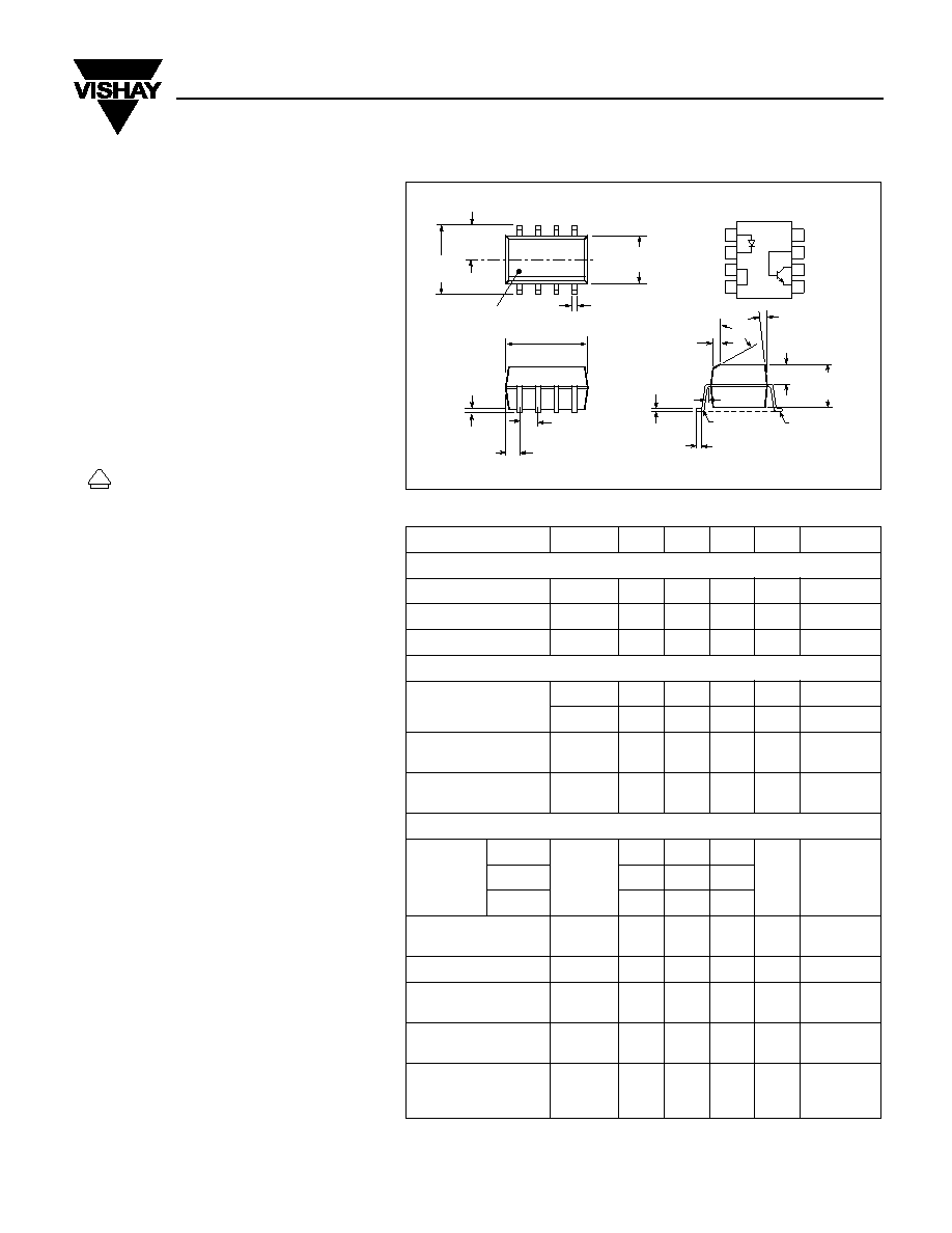
Dimensions in inches (mm)
40
°
.240
(6.10)
.154
±.005
(3.91
±.13)
.050 (1.27)
typ.
.016 (.41)
.192
±.005
(4.88
±.13)
.004 (.10)
.008 (.20)
Lead
Coplanarity
±.0015 (.04)
max.
.015
±.002
(.38
±.05)
.008 (.20)
7
°
.058
±.005
(1.49
±.13)
.125
±.005
(3.18
±.13)
Pin One ID
.120
±.005
(3.05
±.13)
CL
.021 (.53)
5
° max.
R.010
(.25) max.
.020
±.004
(.51
±.10)
2 plcs.
1
2
3
4
Anode
Cathode
NC
8
7
6
5
NC
Base
Collector
Emitter
IL215AT/216AT/217AT
Phototransistor
Small Outline Surface Mount
Optocoupler
相關PDF資料 |
PDF描述 |
|---|---|
| IL255-1 | 1 CHANNEL AC INPUT-TRANSISTOR OUTPUT OPTOCOUPLER |
| IL351T | SPECIALTY OPTOELECTRONIC DEVICE |
| IL352 | 1 CHANNEL TRANSISTOR OUTPUT OPTOCOUPLER |
| IL352-X001 | 1 CHANNEL TRANSISTOR OUTPUT OPTOCOUPLER |
| IL410-X007 | 1 CHANNEL TRIAC OUTPUT WITH ZERO CRSVR OPTOCOUPLER |
相關代理商/技術參數(shù) |
參數(shù)描述 |
|---|---|
| IL217AT | 制造商:Vishay Semiconductors 功能描述:Optocoupler |
| IL217T | 制造商:未知廠家 制造商全稱:未知廠家 功能描述:Optoelectronic |
| IL221 | 制造商:INFINEON 制造商全稱:Infineon Technologies AG 功能描述:PHOTODARLINGTON SMALL OUTLINE SURFACE MOUNT OPTOCOUPLER |
| IL221A | 制造商:INFINEON 制造商全稱:Infineon Technologies AG 功能描述:PHOTODARLINGTON SMALL OUTLINE SURFACE MOUNT OPTOCOUPLER |
| IL221AT | 功能描述:晶體管輸出光電耦合器 Photodarlington Out Single CTR >100% RoHS:否 制造商:Vishay Semiconductors 輸入類型:DC 最大集電極/發(fā)射極電壓:70 V 最大集電極/發(fā)射極飽和電壓:0.4 V 絕緣電壓:5300 Vrms 電流傳遞比:100 % to 200 % 最大正向二極管電壓:1.65 V 最大輸入二極管電流:60 mA 最大集電極電流:100 mA 最大功率耗散:100 mW 最大工作溫度:+ 110 C 最小工作溫度:- 55 C 封裝 / 箱體:DIP-4 封裝:Bulk |
發(fā)布緊急采購,3分鐘左右您將得到回復。