- 您現(xiàn)在的位置:買(mǎi)賣(mài)IC網(wǎng) > PDF目錄360844 > ILC811TU Voltage Detector PDF資料下載
參數(shù)資料
| 型號(hào): | ILC811TU |
| 英文描述: | Voltage Detector |
| 中文描述: | 電壓檢測(cè)器 |
| 文件頁(yè)數(shù): | 2/5頁(yè) |
| 文件大小: | 61K |
| 代理商: | ILC811TU |
ILC811/ILC812 Microprocessor Reset Circuits
October 1999
Impala Linear Corporation
2
(408) 730-3778
www.impalalinear.com
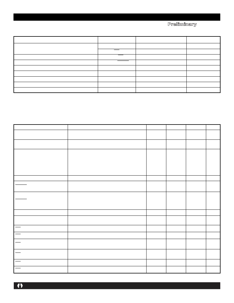
Absolute Maximum Ratings
Stresses above those listed under ABSOLUTE MAXIMUM RATINGS may cause permanent device failure. Functionality at or above these limits is not
implied. Exposure to absolute maximum ratings for extended periods may affect device reliability. Operating ranges define those limits between which the
functionality of the device is guaranteed.
Electrical Characteristics
V
CC
= 5V for ILC81_L/M/J, V
otherwise noted.
CC
= 3.3V for ILC81_S/T, V
CC
= 3V for ILC81_R, T
A
= Operating Temperature Range, unless
Parameter
Symbol
Ratings
Units
Terminal Voltage
V
CC
MR
, MR
-0.3 to 6.0
-0.3 to (V
V
V
CC
+ 0.3)
Input Current
Output Current
Rate of Rise
Operating Temperature Range
Storage Temperature Range
Lead Temperature (Soldering - 10 sec.)
Power Dissipation (T
V
CC
20
20
100
mA
mA
V/μs
°C
°C
°C
mW
RESET, RESET
V
CC
T
A
-40 to +85
-65 to +150
300
320
A
= +70°C)
Parameter
Conditions
Min
1.4
1.6
Typ
Max
5.5
5.5
15
10
4.75
4.50
4.10
3.15
3.00
2.70
560
Units
Operating Voltage Range, V
CC
T
T
ILC811L/M/J, ILC812L/M/J
V
CC
< 3.6V, ILC811R/S/T, ILC812R/S/T
ILC811L, ILC812L
ILC811M, ILC812M
ILC811J, ILC812J
ILC811T, ILC812T
ILC811S, ILC812S
ILC811R, ILC812R
A
A
= 0°C to 70°C
= -40°C to 85°C
V
Supply Current, I
CC
9
6
μA
Reset Voltage Threshold, V
TH
4.50
4.25
3.89
3.00
2.85
2.55
140
– 1.5
0.8 x V
4.63
4.38
4.00
3.08
2.93
2.63
240
V
Reset Timeout Period, t
R
ms
RESET Output Voltage, V
OH
I
I
V
V
V
V
1.8V < V
I
Sink
= 3.2mA, ILC812L/M/J
I
Sink
= 1.2mA, ILC812R/S/T
Source
= 800 μA, ILC811L/M/J
= 500 μA, ILC811R/S/T
= V
TH
Min., I
Sink
CC
= V
TH
Min., I
CC
> 1.4 V, I
Sink
CC
> 1.6 V, I
Sink
< V
TH
V
CC
CC
V
Source
RESET Output Voltage, V
OL
CC
= 3.2 mA, ILC811L/M/J
= 1.2 mA, ILC811R/S/T
= 50 μA, T
A
= 0°C to 70°C
= 50 μA, T
A
= -40°C to 85°C
Min., I
Source
= 150 μA
Sink
0.4
0.3
0.3
0.3
V
RESET Output Voltage, V
OH
CC
0.8 x V
CC
V
RESET Output Voltage, V
OL
0.4
0.3
V
MR Minimum Pulse Width
10
μs
MR to Reset Delay
0.5
μs
MR Input Threshold, V
IH
V
ILC81_R/S/T
CC
> V
TH
Max., ILC81_L/M/J
2.3
0.7 x V
CC
V
MR Input Threshold, V
IL
V
ILC81_R/S/T
CC
> V
TH
Max., ILC81_L/M/J
0.8
0.25 x V
CC
V
MR Pull-Up Resistance
10
20
30
k
MR Glitch Immunity
100
ns
相關(guān)PDF資料 |
PDF描述 |
|---|---|
| ILC812LU | Voltage Detector |
| ILC812MU | Voltage Detector |
| ILC812RU | Voltage Detector |
| ILC812SU | Voltage Detector |
| ILC812TU | Voltage Detector |
相關(guān)代理商/技術(shù)參數(shù) |
參數(shù)描述 |
|---|---|
| ILC812_U | 制造商:IMPALA 制造商全稱(chēng):IMPALA 功能描述:MICROPROCESSOR RESET CIRCUITS |
| ILC812LU | 制造商:未知廠家 制造商全稱(chēng):未知廠家 功能描述:Voltage Detector |
| ILC812MU | 制造商:未知廠家 制造商全稱(chēng):未知廠家 功能描述:Voltage Detector |
| ILC812RU | 制造商:未知廠家 制造商全稱(chēng):未知廠家 功能描述:Voltage Detector |
| ILC812SU | 制造商:未知廠家 制造商全稱(chēng):未知廠家 功能描述:Voltage Detector |
發(fā)布緊急采購(gòu),3分鐘左右您將得到回復(fù)。