- 您現(xiàn)在的位置:買(mǎi)賣(mài)IC網(wǎng) > PDF目錄360844 > ILQ3-2 DARLINGTON-NPN-OUTPUT DC-INPUT OPTOCOUPLER PDF資料下載
參數(shù)資料
| 型號(hào): | ILQ3-2 |
| 英文描述: | DARLINGTON-NPN-OUTPUT DC-INPUT OPTOCOUPLER |
| 中文描述: | 達(dá)林頓- npn型輸出DC -輸入光耦合器 |
| 文件頁(yè)數(shù): | 1/2頁(yè) |
| 文件大小: | 366K |
| 代理商: | ILQ3-2 |
www.infineon.com/opto 1-888-Infineon (1-888-463-4636)
2001 Infineon Technologies Corp. Optoelectronics Division San Jose, CA
2–177
March 8, 2000-01
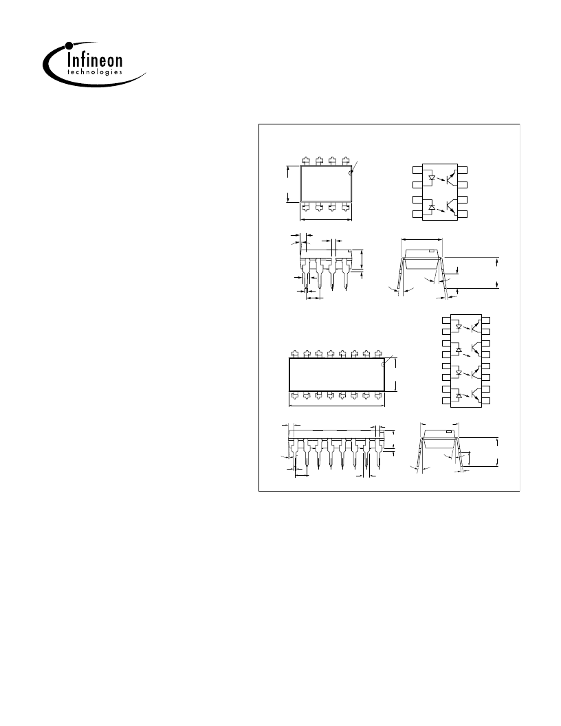
DESCRIPTION
The ILD/Q3 are optically coupled isolated pairs employing GaAs infra-
red LEDs and silicon NPN phototransistor. Signal information, including
a DC level, can be transmitted by the drive while maintaining a high
degree of electrical isolation between input and output. The ILD/Q3 are
especially designed for driving medium-speed logic and can be used
to eliminate troublesome ground loop and noise problems. Also these
couplers can be used to replace relays and transformers in many digi-
tal interface applications such as CRT modulation. The ILD3 has two
isolated channels in a single DIP package and the ILQ3 has four iso-
lated channels per package.
See Appnote 45,
“How to Use Optocoupler Normalized Curves”
.
.255 (6.48)
.265 (6.81)
.779 (19.77 )
.790 (20.07)
.030 (.76)
.045 (1.14)
4
°
.100 (2.54)typ.
10
°
typ.
3
°
–
9
.008 (.20)
.012 (.30)
.018 (.46)
.022 (.56)
.110 (2.79)
.130 (3.30)
pin one ID
.130 (3.30)
.150 (3.81)
.020(.51)
.035 (.89)
8 7 6 5 4 3 2 1
9 10 11 12 13 14 15 16
.031(.79)
.300 (7.62)
typ.
.230 (5.84)
.250 (6.35)
.050 (1.27)
pin one ID
.255 (6.48)
.268 (6.81)
.379 (9.63)
.390 (9.91)
.030 (0.76)
.045 (1.14)
4
°
typ.
.100 (2.54) typ.
10
°
3
°
–
9
°
.008 (.20)
.012 (.30)
.300 (7.62)
typ.
.018 (.46)
.022 (.56)
.110 (2.79)
.130 (3.30)
.130 (3.30)
.150 (3.81)
.020 (.51 )
.035 (.89 )
.230(5.84)
.250(6.35)
4
3
2
1
.031 (0.79)
.050 (1.27)
5
6
7
8
16
15
14
13
12
11
10
9
1
2
3
4
5
6
7
8
Emitter
Collector
Collector
Emitter
Emitter
Collector
Collector
Emitter
Anode
Cathode
Cathode
Anode
Anode
Cathode
Cathode
Anode
1
2
3
4
8
7
6
5
Emitter
Collector
Collector
Emitter
Anode
Cathode
Cathode
Anode
Dimensions in Inches (mm)
Dual Channel
Quad Channel
FEATURES
Current Transfer Ratio at
High Collector-Emitter Voltage
BV
CEO
=50 V
Field-Effect Stable by TRansparent IOn Shield
(TRIOS)
Double Molded Package Offers Isolation Test
Voltage 5300 V
RMS
, 1.0 sec.
Underwriters Lab File #E52744
I
F
=1.6 mA, 300% Min.
Maximum Ratings
Emitter
Reverse Voltage ...................................................6.0 V
Continuous Forward Current ............................. 60 mA
Surge Current...................................................... 2.5 A
Power Dissipation............................................100 mW
Derate Linearly from 25
°
C...........................1.3 mW/
Detector
Collector-Emitter Reverse Voltage.........................50 V
Collector Current............................................... 50 mA
Collector Current (t<1.0 ms)............................ 400 mA
Total Power Dissipation ...................................200 mW
Derate Linearly from 25
°
C...........................2.6 mW/
Package
Isolation Test Voltage (between emitter
and detector, refer to standard climate
23
°
C/50% RH, DIN50014) t=1 sec......... 5300 V
Creepage ......................................................
Clearance......................................................
Isolation Resistance
V
IO
=500 V,
T
A
=25
°
C...............................R
V
IO
=500 V,
T
A
=100
°
C.............................R
Power Dissipation............................................250 mW
Derate Linearly from 25
°
C...........................3.3 mW/
Storage Temperature Range.................
–
40 to +150
Operating Temperature Range..............
–
40 to +100
Junction Temperature.........................................100
Soldering Temperature,
2.0 mm from case bottom...............................260
(Each Channel)
°
C
°
C
RMS
≥
≥
7.0 mm
7.0 mm
IO
IO
=10
=10
12
11
°
°
°
°
C
C
C
C
°
C
DUAL CHANNEL
ILD3
ILQ3
QUAD CHANNEL
Phototransistor
Optocoupler
相關(guān)PDF資料 |
PDF描述 |
|---|---|
| ILD3-2 | DARLINGTON-NPN-OUTPUT DC-INPUT OPTOCOUPLER |
| ILQ32-004 | Optoelectronic |
| ILQ32-009 | Optoelectronic |
| ILD32-004 | Optoelectronic |
| ILD32-009 | Optoelectronic |
相關(guān)代理商/技術(shù)參數(shù) |
參數(shù)描述 |
|---|---|
| ILQ32-004 | 制造商:未知廠家 制造商全稱:未知廠家 功能描述:Optoelectronic |
| ILQ32-009 | 制造商:未知廠家 制造商全稱:未知廠家 功能描述:Optoelectronic |
| ILQ32-X001 | 功能描述:晶體管輸出光電耦合器 Photodarlington Out Quad CTR > 500% RoHS:否 制造商:Vishay Semiconductors 輸入類型:DC 最大集電極/發(fā)射極電壓:70 V 最大集電極/發(fā)射極飽和電壓:0.4 V 絕緣電壓:5300 Vrms 電流傳遞比:100 % to 200 % 最大正向二極管電壓:1.65 V 最大輸入二極管電流:60 mA 最大集電極電流:100 mA 最大功率耗散:100 mW 最大工作溫度:+ 110 C 最小工作溫度:- 55 C 封裝 / 箱體:DIP-4 封裝:Bulk |
| ILQ32-X007 | 功能描述:晶體管輸出光電耦合器 Photodarlington Out Quad CTR > 500% RoHS:否 制造商:Vishay Semiconductors 輸入類型:DC 最大集電極/發(fā)射極電壓:70 V 最大集電極/發(fā)射極飽和電壓:0.4 V 絕緣電壓:5300 Vrms 電流傳遞比:100 % to 200 % 最大正向二極管電壓:1.65 V 最大輸入二極管電流:60 mA 最大集電極電流:100 mA 最大功率耗散:100 mW 最大工作溫度:+ 110 C 最小工作溫度:- 55 C 封裝 / 箱體:DIP-4 封裝:Bulk |
| ILQ32-X007T | 功能描述:晶體管輸出光電耦合器 Photodarlington Out Quad CTR > 500% RoHS:否 制造商:Vishay Semiconductors 輸入類型:DC 最大集電極/發(fā)射極電壓:70 V 最大集電極/發(fā)射極飽和電壓:0.4 V 絕緣電壓:5300 Vrms 電流傳遞比:100 % to 200 % 最大正向二極管電壓:1.65 V 最大輸入二極管電流:60 mA 最大集電極電流:100 mA 最大功率耗散:100 mW 最大工作溫度:+ 110 C 最小工作溫度:- 55 C 封裝 / 箱體:DIP-4 封裝:Bulk |
發(fā)布緊急采購(gòu),3分鐘左右您將得到回復(fù)。