- 您現(xiàn)在的位置:買賣IC網(wǎng) > PDF目錄378631 > IN74LV00 (INTEGRAL JOINT STOCK COMPANY) Quad 2-Input NAND Gate PDF資料下載
參數(shù)資料
| 型號: | IN74LV00 |
| 廠商: | INTEGRAL JOINT STOCK COMPANY |
| 英文描述: | Quad 2-Input NAND Gate |
| 中文描述: | 四2輸入與非門 |
| 文件頁數(shù): | 2/5頁 |
| 文件大小: | 41K |
| 代理商: | IN74LV00 |
IN74LV00
2
INTEGRAL
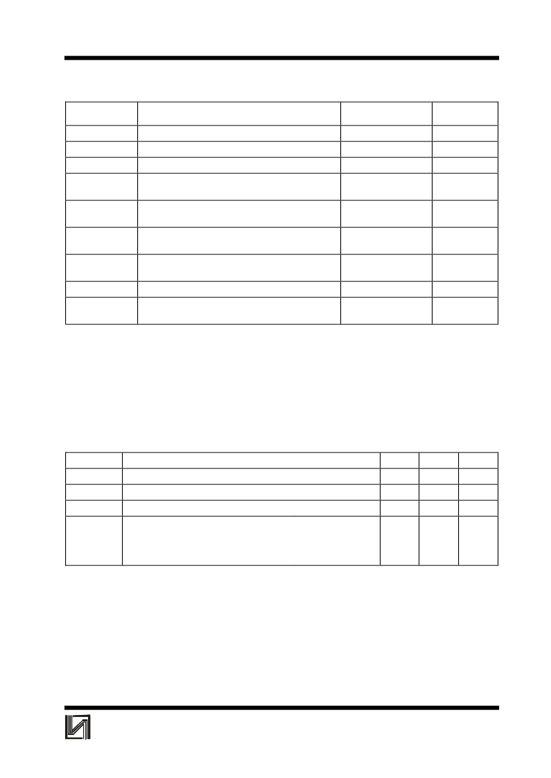
MAXIMUM RATINGS
*
Symbol
Parameter
Value
Unit
V
CC
I
IK
*
1
I
OK
*
2
I
O
*
3
DC supply voltage (Referenced to GND)
-0.5
÷
+5.0
±
20
±
50
±
25
V
DC input diode current
mA
DC output diode current
mA
DC output source or sink current
-bus driver outputs
mA
I
CC
DC V
CC
current for types with
- bus driver outputs
±
50
mA
I
GND
DC GND current for types with
- bus driver outputs
±
50
mA
P
D
Power dissipation per package, plastic DIP+
SOIC package+
750
500
mW
Tstg
Storage temperature
-65
÷
+150
°
C
°
C
T
L
Lead temperature, 1.5 mm from Case for 10 seconds
(Plastic DIP ), 0.3 mm (SOIC Package)
260
*
Maximum Ratings are those values beyond which damage to the device may occur.
Functional operation should be restricted to the Recommended Operating Conditions.
+Derating - Plastic DIP: - 12 mW/
°
C from 70
°
to 125
°
C
SOIC Package: : - 8 mW/
°
C from 70
°
to 125
°
C
*
1
: V
I
<
-0.5 or V
I
>
V
CC
+0.5V
*
2
: Vo
<
-0.5 or Vo
>
V
CC
+0.5V
*
3
: -0.5V
<
Vo
<
V
CC
+0.5V
RECOMMENDED OPERATING CONDITIONS
Symbol
Parameter
Min
Max
Unit
V
CC
DC Supply Voltage (Referenced to GND)
1.2
3.6
V
V
IN
, V
OUT
DC Input Voltage, Output Voltage (Referenced to GND)
0
V
CC
V
T
A
Operating Temperature, All Package Types
-40
+125
°
C
t
r
, t
f
Input Rise and Fall Time
V
CC
=1.2 V
V
CC
=2.0 V
V
CC
=3.0 V
V
CC
=3.6 V
0
0
0
0
1000
700
500
400
ns
This device contains protection circuitry to guard against damage due to high static voltages or electric
fields. However, precautions must be taken to avoid applications of any voltage higher than maximum rated voltages
to this high-impedance circuit. For proper operation, V
IN
and V
OUT
should be constrained to the range GND
≤
(V
IN
or
V
OUT
)
≤
V
CC
.
Unused inputs must always be tied to an appropriate logic voltage level (e.g., either GND or V
CC
). Unused
outputs must be left open.
相關(guān)PDF資料 |
PDF描述 |
|---|---|
| IN74LV00D | Octal Bus Transceivers And Registers With 3-State Outputs 24-SO -40 to 85 |
| IN74LV00N | Octal Bus Transceivers And Registers With 3-State Outputs 24-SO -40 to 85 |
| IN74LV164 | Octal Bus Transceivers And Registers With 3-State Outputs 24-SOIC -40 to 85 |
| IN74LV164D | Octal Bus Transceivers And Registers With 3-State Outputs 24-SOIC -40 to 85 |
| IN74LV164N | Octal Bus Transceivers And Registers With 3-State Outputs 24-SO -40 to 85 |
相關(guān)代理商/技術(shù)參數(shù) |
參數(shù)描述 |
|---|---|
| IN750A-1JANTX | 制造商:ERJ 功能描述: |
| IN750A1JANTXV | 制造商: 功能描述: |
| IN751A | 制造商: 功能描述: 制造商:undefined 功能描述: |
| IN75232 | 制造商:INTEGRAL 制造商全稱:INTEGRAL 功能描述:EIA-232-D INTERFACE 1 CHIP IC |
| IN753ARL | 制造商:n/a 功能描述:SAMPLE |
發(fā)布緊急采購,3分鐘左右您將得到回復(fù)。