- 您現(xiàn)在的位置:買賣IC網(wǎng) > PDF目錄360861 > INA-32063 3.0 GHz Wideband Silicon RFIC Amplifier(3.0 GHz 寬頻帶硅射頻集成電路放大器) PDF資料下載
參數(shù)資料
| 型號(hào): | INA-32063 |
| 英文描述: | 3.0 GHz Wideband Silicon RFIC Amplifier(3.0 GHz 寬頻帶硅射頻集成電路放大器) |
| 中文描述: | 3.0千兆赫寬帶硅射頻放大器(3.0千兆赫寬頻帶硅射頻集成電路放大器) |
| 文件頁(yè)數(shù): | 6/11頁(yè) |
| 文件大小: | 87K |
| 代理商: | INA-32063 |
6
INA-32063 and into the RF Output
pin through the RF choke (RFC).
Capacitor C3 provides RF bypass-
ing for both the V
d
pin and the
power supply end of the RFC.
Capacitor C4 is optional and may
be used to add additional bypass-
ing for the V
d
line. A well-by-
passed V
d
line is especially
necessary in cascades of ampli-
fier stages to prevent oscillation
that may occur as a result of RF
feedback through the power
supply lines.
For this demonstration circuit,
the value chosen for the RF
choke was 120 nH (Coilcraft
1008CS-221, TOKO LL2012 -F or
equivalent). All of the blocking
and bypass capacitors are 100 pF.
The gap in the output transmis-
sion line was bridged using
copper foil cut to size. These
values provide excellent amplifier
performance from under 50 MHz
through 2.4 GHz. Larger values
for the choke and capacitors can
be used to extend the lower end
of the bandwidth. Since the gain
of the INA-32063 extends down to
DC, the frequency response of the
amplifier is limited only by the
values of the capacitors and
choke.
A convenient method for making
RF connection to the demonstra-
tion board is to use a PCB mount-
ing type of SMA connector
(Johnson 142-0701-881, or
equivalent). These connectors
can be slipped over the edge of
the PCB and the center conductor
soldered to the input and output
lines. The ground pins of the
connectors can be soldered to the
ground plane on the backside of
board.
PCB Materials
Typical choices for PCB material
for low cost wireless applications
are FR-4 or G-10 with a thickness
of 0.025 (0.635 mm) or
0.031inches (0.787 mm) A thick-
ness of 0.062 inches (1.574 mm) is
the maximum that is recom-
mended for use with this particu-
lar device. The use of a thicker
board material increases the
inductance of the plated through
vias used for RF grounding and
may deteriorate circuit perfor-
mance. Adequate grounding is
needed not only to obtain maxi-
mum amplifier performance but
also to reduce any possibility of
instability.
Phase Reference Planes
The positions of the reference
planes used to measure S-Param-
eters for this device are shown in
Figure 15. As seen in the illustra-
tion, the reference planes are
located at the point where the
package leads contact the test
circuit.
REFERENCE
PLANES
TEST CIRCUIT
Figure 15. Phase Reference Planes.
SOT-363 PCB Layout
The INA-32063 is packaged in the
miniature SOT-363 (SC-70)
surface mount package. A PCB
pad layout for the SOT-363
package is shown in Figure 16
(dimensions are in inches). This
layout provides ample allowance
for package placement by auto-
mated assembly equipment
without adding pad parasitics that
could impair the high frequency
performance of the INA-32063.
The layout that is shown with a
nominal SOT-363 package foot-
print superimposed on the PCB
pads for reference.
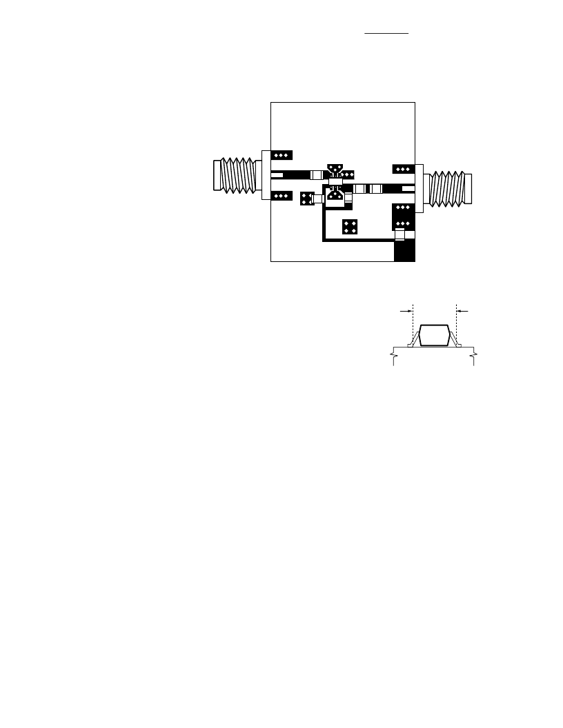
C2
RFC
C1
C3
C4
V
d
INA-3XX63 DEMO BOARD
3
Figure 14. Assembled Amplifier.
相關(guān)PDF資料 |
PDF描述 |
|---|---|
| INA-34063 | 3.0 GHz Medium Power Silicon RFIC Amplifier(3.0 GHz中等功率硅射頻集成電路放大器) |
| INA-50311 | 1 GHz Low Noise Silicon MMIC Amplifier |
| INA-50311-BLK | 1 GHz Low Noise Silicon MMIC Amplifier |
| INA-50311-TR1 | 1 GHz Low Noise Silicon MMIC Amplifier |
| INA-51063 | 2.4 GHz Low Noise Silicon MMIC Amplifier |
相關(guān)代理商/技術(shù)參數(shù) |
參數(shù)描述 |
|---|---|
| INA-32063-BLK | 制造商:AGILENT 制造商全稱:AGILENT 功能描述:3.0 GHz Wideband Silicon RFIC Amplifier |
| INA-32063-TR1 | 制造商:AGILENT 制造商全稱:AGILENT 功能描述:3.0 GHz Wideband Silicon RFIC Amplifier |
| INA-32063-TR2 | 制造商:AGILENT 制造商全稱:AGILENT 功能描述:3.0 GHz Wideband Silicon RFIC Amplifier |
| INA321 | 制造商:TI 制造商全稱:Texas Instruments 功能描述:microPower, Single-Supply, CMOS Instrumentation Amplifier |
| INA321E | 制造商:Texas Instruments 功能描述:AMP INSTRUMENTATION VSSOP8 321 |
發(fā)布緊急采購(gòu),3分鐘左右您將得到回復(fù)。