- 您現(xiàn)在的位置:買賣IC網(wǎng) > PDF目錄360861 > INA104 Very-High Accuracy INSTRUMENTATION AMPLIFIER PDF資料下載
參數(shù)資料
| 型號(hào): | INA104 |
| 元件分類: | 測(cè)量放大器 |
| 英文描述: | Very-High Accuracy INSTRUMENTATION AMPLIFIER |
| 中文描述: | 甚高精度儀表放大器 |
| 文件頁數(shù): | 7/11頁 |
| 文件大?。?/td> | 132K |
| 代理商: | INA104 |
7
INA104
DISCUSSION
OF PERFORMANCE
INSTRUMENTATION AMPLIFIERS
Instrumentation amplifiers are closed-loop gain blocks whose
committed circuitry accurately amplifies the voltage applied
to their inputs. They respond only to the difference between
the two input signals and exhibit extremely high input imped-
ance, both differentially and common-mode. Feedback net-
works are packaged within the amplifier module. Only one
external gain setting resistor must be added. An operational
amplifier, on the other hand, is an open-loop, uncommitted
device that requires external networks to close the loop.
While operational amplifiers can be used to achieve the same
basic function as instrumentation amplifiers, it is difficult to
reach the same level of performance. Using operational
amplifiers often leads to design trade-offs when it is neces-
sary to amplify low level signals in the presence of common-
mode voltages while maintaining high input impedances.
THE INA104
A simplified schematic of the INA104 is shown on the front
pages of this data sheet. It is a three-amplifier device which
provides all the desirable characteristics of a premium per-
formance instrumentation amplifier. In addition, it has fea-
tures not normally found on integrated circuit instrumenta-
tion amplifiers.
The input section (A
1
and A
2
) incorporates high perfor-
mance, low drift amplifier circuitry. The amplifiers are
connected in the non-inverting configuration to provide the
high input impedance (10
10
) desirable in the instrumenta-
tion amplifier function. The offset voltage and offset voltage
versus temperature is low due to the monolithic design and
improved even further by the state-of-the-art, laser-trimming
techniques.
The output section (A
3
) is connected in a unity-gain differ-
ence amplifier configuration. A critical part of this stage is
the matching of the four 10k
resistors which provide the
difference function. These resistors must be initially well
matched and the matching must be maintained over tem-
perature and time in order to retain excellent common-mode
rejection. (The 106dB minimum at 60Hz for gains greater
than 100V/V is a significant improvement compared to most
other integrated circuit instrumentation amplifiers.)
All of the internal resistors are compatible, thin-film nichrome
formed with the integrated circuit. The critical resistors are
laser-trimmed to provide the desired high gain accuracy and
common-mode rejection. Nichrome ensures long-term sta-
bility of trimmed resistors and excellent TCR and TCR
tracking. This provides gain accuracy and common-mode
rejection when the INA104 is operated over wide tempera-
ture ranges.
The fourth op amp (A
4
) of the INA104 adds a great deal of
versatility and convenience to the amplifier. It allows easy
implementation of active low-pass filtering, output offset-
ting, and additional gain generation. The pin connections
make the use of this stage optional and the specifications
appear separately in the table of Specifications.
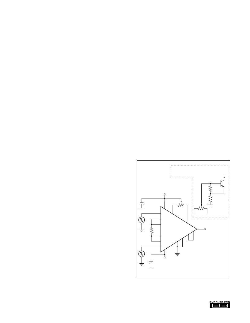
USING THE INA104
Figure 1 shows the simplest configuration of the
INA104. The gain is set by the external resistor, R
G
,
with a gain equation of G = 1 + (40k/R
G
). The
accuracy and TCR of R
G
contribute directly to the gain
accuracy and drift.
For gains greater than unity, resistor R
G
is connected
between pins 5 and 14. At high gains, where the value of
R
G
becomes small, additional resistance (i.e., relays,
sockets) in series with R
G
will contribute to gain error.
Care should be taken to minimize this effect. However,
this error can be virtually eliminated with the INA104 by
using the Gain Sense circuit connection.
Pins 1, 5, 14, and 18 are accessible so that a four-
terminal connection can be made to R
G
. (Pins 1 and 18
are the voltage sense terminals, since no signal current
flows into the operational amplifiers’ inputs.) This is
useful at high gains, where the value of R
G
is small.
The optional offset adjust capability is shown in
Figure 1. The adjustment affects only the input stage
component of the offset voltage. Thus, the null con-
dition will be disturbed (if input offset is not adjusted
to zero) when the gain is changed. Also, the input
drift will be affected by approximately 0.31
μ
V/
°
C
per 100
μ
V of input offset voltage that is trimmed.
Therefore, care should be taken when considering use
of the control for removal of other sources of offset.
FIGURE 1. Basic Connection for the INA104 Including
Optional Input Offset Null Potentiometer.
3
7
10
11
6
8
13
15
16
17
18
14
5
1
2
INA104
R
G
100k
E
OUT
E
1
E
2
+V
CC
–V
CC
(1)
1μF
Tantalum
1μF
Tantalum
NOTE: (1) Connect pin 7 to common and pin 10
to pin 11 when Internal Amp A
4
is not used.
Gain Sense
Gain Sense
Optional
Offset
Adjust
This circuit may be used as replacement for
the single potentiometer. It will adjust offset
and leave drift unchanged.
+V
CC
15
16
100k
10M
2M
E
OUT
= [1 = (40k/R
G
)] (E
2
– E
1
)
–In
+In
2N2222
相關(guān)PDF資料 |
PDF描述 |
|---|---|
| INA104AM | RES THKF 0805 .125W 5% 680 OHM ROHS |
| INA104BM | Very-High Accuracy INSTRUMENTATION AMPLIFIER |
| INA104CM | Very-High Accuracy INSTRUMENTATION AMPLIFIER |
| INA104SM | Very-High Accuracy INSTRUMENTATION AMPLIFIER |
| INA104 | Very-High Accuracy Instrumentation Amplifier(非常高精度的儀用放大器) |
相關(guān)代理商/技術(shù)參數(shù) |
參數(shù)描述 |
|---|---|
| INA104AM | 制造商:BB 制造商全稱:BB 功能描述:Very-High Accuracy INSTRUMENTATION AMPLIFIER |
| IN-A-104B-H/MS-PC-212 | 制造商:Hirose 功能描述:901-1090-9-00 EACH 制造商:Hirose 功能描述:IN-A-104B-H/MS-PC-212 |
| INA104BM | 制造商:BB 制造商全稱:BB 功能描述:Very-High Accuracy INSTRUMENTATION AMPLIFIER |
| INA104CM | 制造商:BB 制造商全稱:BB 功能描述:Very-High Accuracy INSTRUMENTATION AMPLIFIER |
| INA104SM | 制造商:BB 制造商全稱:BB 功能描述:Very-High Accuracy INSTRUMENTATION AMPLIFIER |
發(fā)布緊急采購,3分鐘左右您將得到回復(fù)。